Memory
This page provides some technical and historical background on the various types and sizes of memory that were used in DOS computers, both on the motherboard and on graphics cards.
Before we delve into the different formats of memory chips and memory modules, it is important to understand the structure of memory used by DOS as well as some terminology.
DOS Memory Allocation
 By default, DOS can only "see" the first 640 KB of memory (from 0 KB up to 640 KB) - this is called Conventional Memory, or Base Memory. No drivers need to be loaded to have access to all of this.
A common problem however is that DOS itself, by default, installs itself into this area of memory, leaving you with a smaller amount available for your own programs.
In the original design of the IBM PC, the area of memory above 640 KB and below 1 MB (called the Upper Memory Area) was reserved for use as video memory, the ROM BIOS, Video BIOS, and extra space to be used by hardware manufacturers for 'option ROMs'.
As time went on, however, it became apparent a lot of unused space still existed in this area, so the use of Upper Memory Blocks (UMBs) for programs came into being. Since DOS isn't even aware this area of memory exists, you needed to ensure HIMEM.SYS (a memory manager supplied with DOS) was loaded in your CONFIG.SYS file.
The primary purpose of HIMEM.SYS wasn't primarily to open up UMBs for use - it was to expose DOS to the 64 KB that sits just above the 1 MB mark - this is called the High Memory Area. When the command DOS=HIGH is seen in your CONFIG.SYS file (after your HIMEM.SYS line), DOS will attempt to load itself into this High Memory Area, keeping as much of your precious conventional memory available as possible. Other programs could also use the High Memory Area if programmed to do so. If your command is DOS=HIGH,UMB it will do the same thing, but also create a series of UMBs in the Upper Memory Area. You can then use the CONFIG.SYS command DEVICEHIGH=<device driver> and the AUTOEXEC.BAT command LOADHIGH <program> to install those device drivers or programs into the UMBs. There are other memory managers aside from HIMEM.SYS to allow you to gain access to the Upper Memory Area. Especially important for 286 systems, some BIOS manufacturers created their own UMB memory manager to allow for the use of the Upper Memory Area.
CPUs and Memory They Can Use
| CPU | Max Mem | UMBs | XMS | EMS |
|---|---|---|---|---|
| 808x | 1 MB | *1 | No | No |
| 80286 | 16 MB | Yes | Yes | *2 |
| 80386 | 4 GB | Yes | Yes | Yes |
*1: XT-class machines require hardware or firmware to support UMBs.
*2: 80286s can use EMS if your chipset supports it and you have the proprietary driver, e.g. the Headland HT12P-16/a, but the EMM386 memory manager requires a 386.
All the memory in your system above the High Memory Area is called Extended Memory. Like the Upper and Higher Memory Areas, by default this is not usable without installing a memory manager. For 386 systems and above, DOS came with EMM386.SYS (later called EMM386.EXE). This opened up this memory to be accessible by programs written in alignment with one of two standards that were created: the Extended Memory Specification (XMS) and Expanded Memory Specification (EMS). Both of these achieved the same end result, but went about it in different ways. XMS took the 384 KB Upper Memory Area and used it as a 'window' into the much larger block of memory above 1 MB. EMS split up the Extended Memory into blocks called page frames which would be paged in and out of conventional memory to be read/written to. EMM386 was the XMS/EMS memory manager that came with DOS. You could configure your extended memory as XMS by having the line DEVICE=EMM386.EXE NOEMS in your CONFIG.SYS file. If you wanted EMS memory instead, you would use DEVICE=EMM386.EXE RAM. There were numerous other arguments you could add to these to further fine-tune the memory configuration. You could also have a combination of XMS and EMS available. By default if you didn't assign the entire amount of memory available in the Extended Memory area to EMS, what remained would be available as XMS.
Note that the DOS version is important when using memory managers:
- The ability to use DOS=HIGH only arrived in DOS 4.0 (released in 1991).
- EMM386.SYS was renamed EMM386.EXE in DOS 5.0 (1991).
Memory Chip Terminology
Sometimes when we talk about memory modules (a collection of memory chips grouped together), there are certain terms that are used. These are described below:
Memory Density
This is the total memory capacity of the chip. Example: 128 MB (megabytes).
Memory Depth × Memory Width
Memory Depth is the Memory Density divided by Memory Width.
Example: A memory chip with 128 MB (megabytes) capacity and 8 bit wide data bus can be specified as: 16 Meg × 8. Sometimes the "Meg" or "Mi" is dropped, as in 16×8.
(Memory Depth per bank × Memory Width) × Number of Banks
Example: a chip with the same capacity and memory width as above but constructed with 4 banks would be specified as (4 MB x 8) x 4.
Note that there are two sizes of RAM chip; 256Kbit (kilobit) and 1Mbit (megabit). It is important to distinguish between bits and bytes here. The "bit" measurement is for individual chips, the "byte" measurement is for memory size.
All the RAM chips function in sets of eight (or nine with parity) whether
they are installed individually or are part of a module. The individual chip measurement e.g. 256Kbit, represents the total amount
of memory in one set of eight (or nine chips). Eight or Nine 256Kbit chips will therefore total 256K bytes (kilobytes) of memory and eight (or nine) 1Mbit chips will total 1MB (megabyte).
Only one size chip can be used in any one bank.
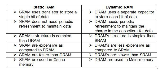
SRAM (Cache chips)
The first caches on DOS PCs started to appear on later 80386-based motherboards. Since the 386DX or 386SX didn't come with any cache on the CPU die itself, this motherboard-based cache would typically provide a boost in overall system performance. Cache sizes started at 64 KB and went up to 512 KB. Some CPUs made by Cyrix (Cx486DLC/DRx2), IBM (IBM DLC3) and Texas Instruments (TI486DLC/SXL) that were compatible with 386/486 hybrid motherboards came with a small on-die cache of 1 KB, 8 KB or 16 KB.
With the introduction of the 80486 CPU, the concept of L1 (level 1) and L2 (level 2) caches arrived. Whilst L1 cache was on the CPU itself, L2 cache was a set of chips on the motherboard. Sometimes they are referred to as Internal Cache and External Cache These are typically SRAM (Static Random Access Memory) chips and are the fastest RAM chips.
To see the differences between SRAM and DRAM:
DRAM
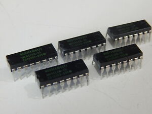 Before there were memory modules (or "sticks"), we simply plugged individual Dynamic RAM "DIP" chips directly into sockets on the board. Each chip would typically store anywhere from 16 KB up to 128 KB. DRAM chips were very common from the first IBM PC, through to the XT, and early AT machines, with some budget 386 boards still supporting DRAMs alongside SIPP sockets in 1992.
DRAMs were always stamped with a speed rating, which refers to the time it takes for the chip to read, modify and write some data. Typical DRAM chips came in speeds from 150 nanoseconds (150ns) at the slower end of the spectrum, to 60 nanoseconds (60ns) at the fastest.
SIPP
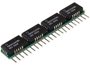 SIPPs (Single Inline Pin Packages) allowed motherboard manufacturers to store larger amounts of memory on modules, rather than via individual DRAM ICs.
They are comprised of chips mounted in a set on a strip that plugs in as a unit. SIPs pre-date SIMMs as a means of grouping memory chips together. SIPPs had their heyday during the 80286 era. I have never seen a SIPP socket on an XT motherboard (probably because XTs were limited to 640 KB in most cases), but my late 80286 motherboard from 1992 has them.
SIPP modules had 30 pins that plugged into matching holes in the motherboard, and are pin-compatible with the later 30-pin SIMMs.
SIPP modules came in two sizes depending on which size chip they use. One SIPP module can total either 256 KB or 1 MB. Around 1990 SIPPs were succeeded by the more durable SIMM design.
I have permission to link to Martin @ Marten Electric's awesome SIMM/SIPP module database - do check it out if you're struggling to identify any of your modules!
SIMM
30-pin SIMM
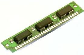 SIMM cards came in around 1989, overlapping the period when SIPPs were still around. It was not uncommon to have SIMM slots and DRAM sockets on the same motherboard, just as it was common to have SIPPs alongside DRAMs too.
The first SIMMs (Single Inline Memory Module) had 30 pins (the same as the SIPPs they directly replaced), with either a tin or gold edge connector - this made them less prone to breaking than SIPPs. The edge connector contacts are redundant on both sides of the module (their opposite pin does the same thing). The physical size of a 30-pin SIMM is approximately 3.5 x .75 inches (about 9 x 2 cm). They are also 'keyed' to prevent insertion the wrong way around in a slot.
These SIMMs provide 8 bits of data plus a 9th error-detection bit in the case of parity SIMM modules. These were used in AT-compatible (286-based, 386-based, and 486-based) computers, as well as the Atari ST and numerous early Apple Macintosh computers. In the early days, module capacities were just 256 KB and 1 MB, but as memory technology improved and costs reduced, 4 MB and even 16 MB 30-pin SIMMs were produced.
During the time of 30-pin SIMMs, parity became supported by motherboards and their BIOS. For memory modules with parity, the DRAM controller would store a checksum (for error checking) of what had been written, and read it back to ensure what had been stored was 100% accurate.
All 30-pin SIMMs use the "Fast Page Mode" (FPM) DRAM technology.
: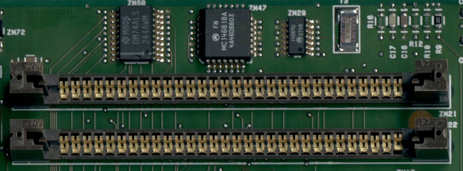
Two 30-pin SIMM slots on a motherboard. Installation of a 30-pin SIMM [in the case above] is vertical, using the two black plastic end-guides to ensure it goes in correctly. Most SIMM slots use a different design where the module is inserted at a slight angle (about 30 degrees) and then tilted vertically until it snaps into place via two metal springs on each end of the slot.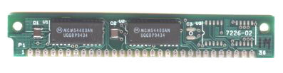
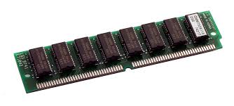
A 30-pin SIMM with a tin edge connector, and holds 256 KB of RAM. It has 100ns (nanosecond) DRAM chips, with no parity
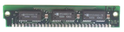
A 3-chip module that has 1 MB of RAM, and uses 70ns chips with parity
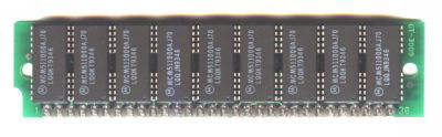
A 9-chip module that has 1 MB of RAM with 70ns chips with parity
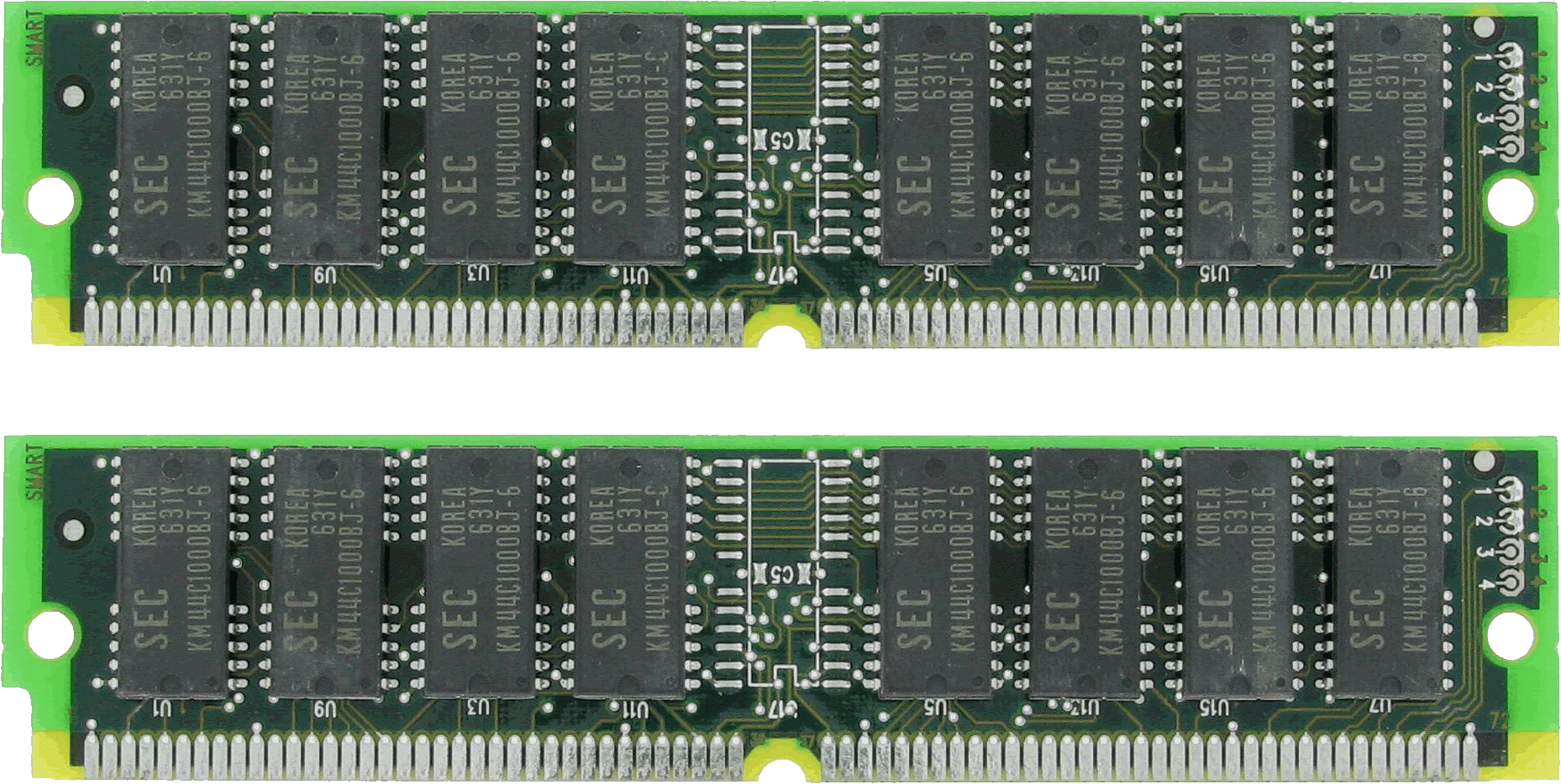
Because 30-pin SIMMs were 8-bits wide, you would need two of them to fill a memory "bank" on 16-bit systems (80286 and 80386SX). This 'banking' was necessary due to the different data bus widths that existed between processors and their motherboards. For 32-bit systems (386DX, i486, etc), a bank would require four of these 8-bit-wide 30-pin SIMMs to be filled (4 x 8 = 32). The golden rule with 30-pin SIMM slots is that all slots in a single bank are populated - what a motherboards calls a "bank" differs depending on whether it supports memory interleaving or not.
A Word on Memory Interleaving
Some 286-, 386- and 486-based systems used what was known as "memory interleaving", where it would split the memory into two to permit parallel access - this would result in great performance improvements on memory read operations. A fast 286 motherboard that supported interleaving would usually accept slower RAM (100 or 120ns), but without interleaving it would require 60-80ns RAM to achieve decent throughput.
You can usually tell if a SIMM module supports parity (error) checking or not by how many chips there are. If it's an odd number, you have a parity SIMM. If it's an even number, it's non-parity.
30-pin SIMMs ranged from 60ns (nanoseconds) to 100ns, with 70ns being the most common - the smaller the number, the faster the memory can operate. Bear in mind the speed stamped on each memory chip denotes the MAXIMUM speed that chip can run at - your ACTUAL memory speed is affected by your BIOS [memory timing and wait state] settings and your motherboard's chipset (some are faster/more efficient than others). To ensure system stability all SIMMs installed in a motherboard should be the same speed, ideally from the same manufacturer, and don't mix parity with non-parity SIMMs. Parity SIMMs tend to be those with an odd number of chips while non-parity tend to be an even number of chips.
I have permission to link to Martin @ Marten Electric's awesome SIMM/SIPP module database - do check it out if you're struggling to identify any of your modules!
72-pin SIMM
 The second variant of SIMMs has 72 pins, and provides 32 bits of data (36 bits in parity versions). These appeared in the early 1990s in the IBM PS/2, and later in systems based on the 486, Pentium, Pentium Pro, and early Pentium II era. By the mid-90s, 72-pin SIMMs had completely replaced 30-pin SIMMs in new-build computers, and were starting to be replaced themselves by DIMMs (see below). Physically a 72-pin is approximately 4.25 x 1 inch (about 110 x 25mm). To ensure that a 72-pin SIMM is correctly installed in a memory slot, there is a notch next to pin 1 (seen on the far right in the picture above).
The earlier 72-pin SIMMs continued to use Fast Page Mode (FPM) DRAM technology. This was slow, and as technology progressed, higher performance EDO (Extended Data Out) DRAM technology was used in later 72-pin modules. This had more advanced timing features, extending the amount of time data could be stored and had a reduced refresh rate which alleviated the CPU and RAM from timing constraints and improved performance.
Capacities of 72-pin SIMMs started at 1 MB and rose gradually up to 128 MB, with versions that held 2 MB, 4 MB, 8 MB, 16 MB, 32 MB and 64 MB in between.
Typically, a single 72-pin SIMM was required to fill a memory bank on 32-bit systems such as the 80386DX, or i486. For Pentium-class systems (which had a 64-bit data bus), two 72-pin SIMMs were required to fill a bank.
With 72-pin SIMMs also came the first more intelligent means of a motherboard identifying what was installed. The JEDEC standard on which the 72-pin SIMM was based called for a number of 'Presence Detect' pins on the memory board to allow motherboards to recognise the board's capacity and speed.
Two 72-pin SIMMs, each holding 64 MB (making up a bank that has 128 MB). These use the older FPM DRAM technology, and have parity.
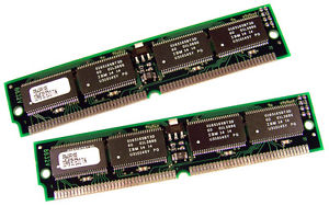
64 MB (2 sticks of 32 MB each) EDO SIMM. The chips are 8 Mbit x 32.
72-pin SIMMs ranged from 60ns (nanoseconds) to 70ns, with 70ns being the most common for FPM RAM and 60ns for EDO.
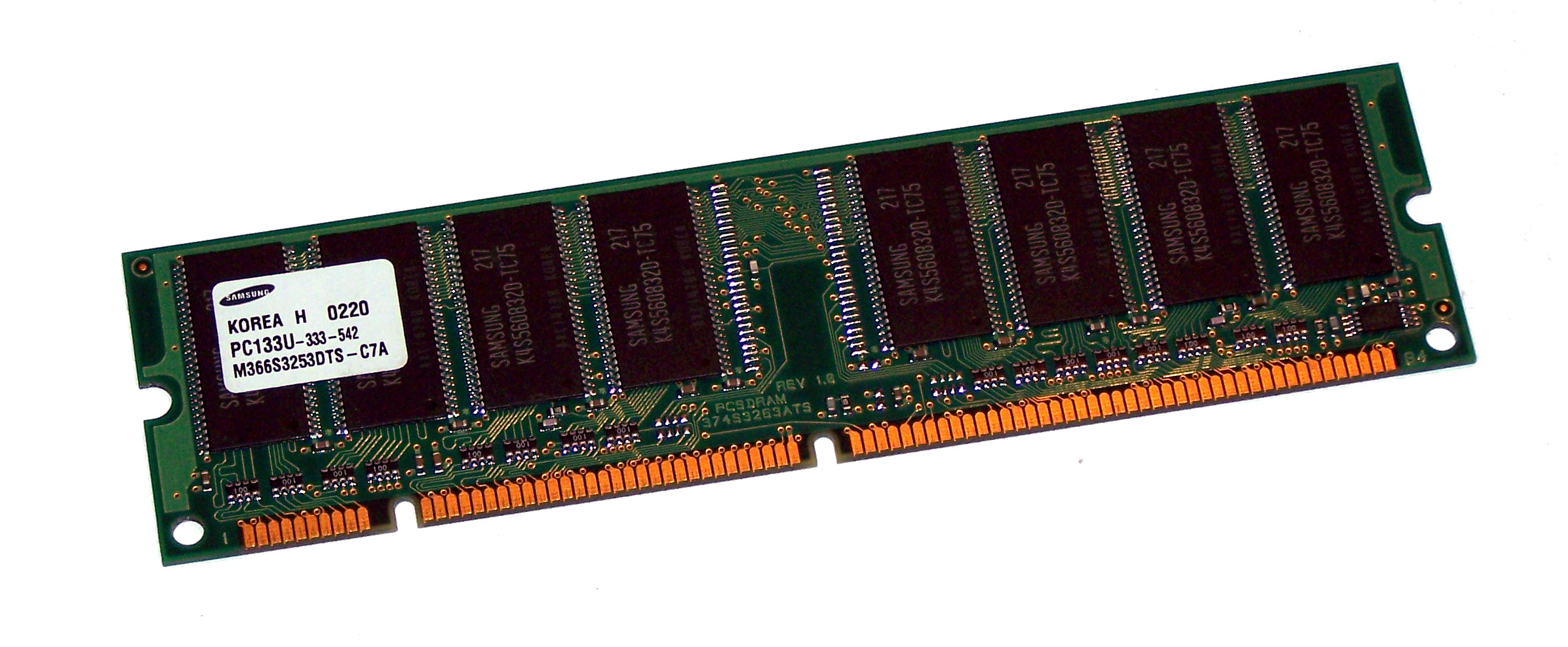
DIMM
 The third type of memory for PCs (chronologically) was DIMMs - Dual Inline Memory Modules. They began to take over from 72-pin SIMMs during the later Pentium era (around 1996). The limitation with SIMMs was that they were designed for a 32-bit data bus width. On systems with a 64-bit data bus, SIMMs were installed in matching pairs and the CPU would access the two SIMMs in parallel. DIMMs were introduced to eliminate this limitation (no more "banks" of memory).
Physically a DIMM is approximately 133mm x 40mm in size. DIMM modules for laptop computers were also introduced, called SODIMM - these are about half the length of a DIMM module.
The first DIMMs had 168 pins, 84 on each side, so both sides' pins were not redundant as with SIMMs. They all have a "voltage-alignment key" notch which is used in a different location depending on the technology used on that memory stick. Initially the technology used with DIMMs was SDRAM (Synchronised Dynamic RAM) - this was significantly faster than FPM and even EDO RAM - if your Super Socket 7 motherboard's chipset supported SDRAM you had . With SDRAM the memory was synchronised with the system bus/clock speed, so it could run at faster speeds (up to around 133 MHz) than the older unsynchronised DRAM. A problem that was becoming more prevalent with DRAM was that the memory couldn't keep up with the demands being made upon it by the CPU. By running synchronously, it could queue up one instruction while processing another. This was later referred to a SDR (Single Data Rate) SDRAM when DDR (Double Data Rate) SDRAM arrived.
Due to the ubiquity of the DIMM form factor over a long time frame, DIMM modules started to be referred to not just by their size but also the speed of the bus they could run on. For example, a 256 MB SDRAM PC133 DIMM 168-pin memory module contains 256 MB of RAM, it uses the SDRAM technology, and supports a front side bus speed of 133 MHz.
The DIMM form factor was continued for many years into the new milennium, with the introduction of DDR (Double Data Rate) RAM in June 2000 which made faster data transfer rates possible, and later DDR2 (mid-2003 with Intel's introduction of their 9xxx series of chipsets), DDR3 (2007) and DDR4 (2014). All used the faster SDRAM technology.
None of these are forward- or backward-compatible with each other, and motherboards support only one of these types of DIMM module. Having said that, within a single module's technology, speeds are interchangeable. For example:
a PC133 DDR DIMM module on a motherboard that supports PC133 DDR modules = OK, and runs at 133 MHz.
a PC100 DDR DIMM module on a motherboard that supports PC133 DDR modules = OK, and runs at 100 MHz.
a PC133 DDR DIMM module on a motherboard that supports only PC100 DDR modules = OK, and also runs at 100 MHz.
In other words the memory cannot run faster than the slowest element, either motherboard limitation or memory module limitation.
DDR Module Terminology
From 1996, JEDEC set standards for DDR SDRAM memory modules and their names to allow people to ensure compatibility across the industry and to give consumers an understanding of peak memory transfer rates, as follows:-
| Technology | Year It Went Mainstream | Standard Name | Module Name | Peak Transfer Rate |
|---|---|---|---|---|
| DDR SDRAM (1997) | 1998 | DDR-200 | PC-1600 | 1600 MB/sec |
| 1999 | DDR-266 | PC-2100 | 2133.33 MB/sec | |
| 2000 | DDR-333 | PC-2700 | 2666.67 MB/sec | |
| 2002 | DDR-400 | PC-3200 | 3200 MB/sec | |
| DDR2 SDRAM (2003) | 2004 | DDR2-400 | PC2-3200 | 3200 MB/sec |
| 2005 | DDR2-533 | PC2-4200 | 4266.67 MB/sec | |
| 2007 | DDR2-667 | PC2-5300 | 5333.33 MB/sec | |
| 2008 | DDR2-800 | PC2-6400 | 6400 MB/sec | |
| 2008 | DDR2-1066 | PC2-8500 | 8533.33 MB/sec | |
| DDR3 SDRAM (2007) | 2007 | DDR3-800 | PC3-6400 | 6400 MB/sec |
| 2008 | DDR3-1066 | PC3-8500 | 8533.33 MB/sec | |
| 2009 | DDR3-1333 | PC3-10600 | 10667 MB/sec | |
| 2010 | DDR3-1600 | PC3-12800 | 12800 MB/sec | |
| 2010 | DDR3-1800 | PC3-15000 | 15000 MB/sec | |
| 2011 | DDR3-2000 | PC3-16000 | 16000 MB/sec |
Memory Technology Used by Graphics Cards
FPM and EDO DRAM
For all of the 1980s, graphics cards used exactly the same type of memory as that found on PC motherboards - DRAM chips. In the early 90s the introduction of 72-pin SIMMs for main system memory also brought in the new EDO (Extended Data Out) DRAM technology. Graphics cards soon started making use of the same underlying EDO DRAM ICs on their cards.
VRAM
In 1991, Texas Instruments pioneered the first VRAM (video RAM) technology, and these became more commonly used on more expensive graphics cards. VRAM is dual-port memory technology (the ability to fetch the contents of memory for display at the same time that new bytes are being pumped into memory) and was quite expensive, requiring special technology in the memory controllers. The first port, the DRAM port, behaved in much the same way as standard DRAMs. The second port, the video port, was typically read-only and was dedicated to providing a high throughput serialized data channel for the graphics chipset. Through the 1990s, many graphic subsystems used VRAM, with the number of megabits touted as a selling point.
WRAM
In 1995, Samsung came out with a newer, less expensive WRAM (Window RAM, unrelated to Microsoft’s Windows), which was a further development on VRAM that came before it. WRAM was a high-performance dual-ported video RAM that had about 25% more bandwidth than VRAM. It had features that made it more efficient to read data for use in block fills and text drawing and could be used for very high resolution (such as 1600 × 1200) using true color. WRAM was cheaper than VRAM, despite it being better/faster. It was only used by Matrox (for their Millennium and Millennium II), Number Nine (for their Revolution 3D) and ATi (for their 3D Rage Pro). Because it was patented, Samsung did not release the specs for others to build their own WRAM chips - this caused a chip shortage for WRAM and ultimately, its reduced adoption.
MDRAM
Multibank DRAM (MDRAM) is a type of specialized DRAM developed by MoSys. It is constructed from small memory banks of 256 kB, which are operated in an interleaved fashion, providing bandwidths suitable for graphics cards at a lower cost to memories such as SRAM. It was used on cards such as those based on the Tseng Labs ET6000. Boards based upon this chipset often had the unusual capacity of 2.25 MB because of MDRAM's ability to be implemented more easily with such capacities. A graphics card with 2.25 MB of MDRAM had enough memory to provide 24-bit color at a resolution of 1024×768—a very popular setting at the time.
SDRAM
In the late 1990s, SDRAM technology gradually became affordable, dense, and fast enough to displace VRAM. It had been around for a long time, but up to this point didn't see widespread use in graphics adapters due to cost.
It was only single-ported and more overhead was required than that of VRAM and WRAM. Nevertheless, many of the VRAM concepts of internal, on-chip buffering and organization have been used and improved in modern graphics adapters.
SGRAM
Synchronous graphics RAM (SGRAM) was a specialized form of SDRAM for graphics adaptors. It added functions such as bit masking (writing to a specified bit plane without affecting the others) and block write (filling a block of memory with a single colour). Unlike VRAM and WRAM, SGRAM was single-ported. However, it could open two memory pages at once, which simulated the dual-port nature of other video RAM technologies.
GDDR
In 2000, GDDR memory was introduced, making both VRAM and WRAM obsolete.