386 Motherboard Repair - Part 2
In Part 1, I introduced you to my favourite and now-broken 386 motherboard. We started preliminary troubleshooting by checking the power supply inputs, reset circuit, and whether we were getting a clock signal.
In this Part 2, we'll continue our troubleshooting...
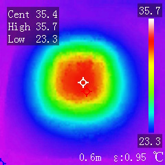
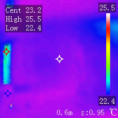
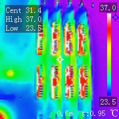
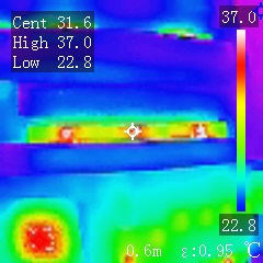
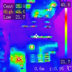
7) Check for hot chips
I used a basic infra-red sensor to determine which components were running hot. This can be a very quick way to see if any major or minor "glue logic" ICs such as buffers or logic gates aren't getting any power at all or have an internal fault, since most will get at least a little bit warm when power is applied.
| Bad Board | Good Board | |
|---|---|---|
| Am386DX-40 (on bad board the PQFP is on the left, PGA right) | 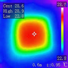 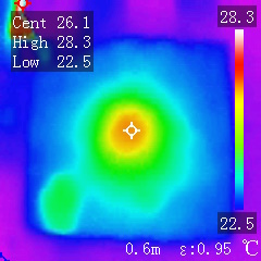 |
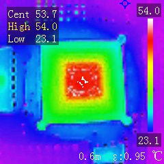 |
| OPTi 82C495XLC | 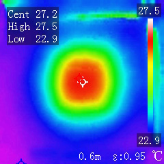 |
 |
| OPTi 82C208 | 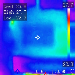 |
 |
| Main Memory | 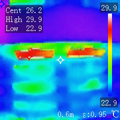 |
 |
| Buffers/Latches | 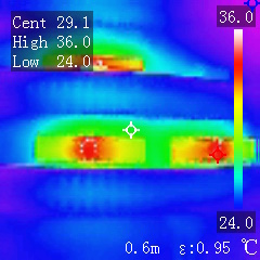 |
 |
| Entire board | 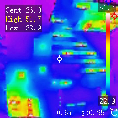 |
 |
a) 82C206 Periperhal Controller is just a very cool chip.
b) On the bad board, the PQFP CPU is still powered up and in an active state even if the PGA is installed and configured for use.
c) The PGA version runs a bit cooler than the PQFP version.
d) Only one of the SIMMs appears to be showing signs of life on the bad board - this is known-good memory taken out of the good board and installed in the bad board - 4 SIMMs of 1 MB each. I checked every trace connecting all the SIMM slots on the rear of the board and all were connected, implying we have no cut or damaged traces.
8) Is the CPU faulty?
I'm not yet ready to delve into checking signals - the first thing now is to see if the soldered-in Am386DX CPU is faulty, and since I already installed a PGA-132 socket to this motherboard, I'm going to try a known-good 80386DX CPU in there and configure the board's jumpers accordingly.
There's no info on what this means for an MR BIOS. If this were an AMI or Award BIOS, C5 means the 'early shadow-RAM enable for faster boot' and this occurs wayyy down the list of POST checks. I see no series of earlier POST codes being displayed, so I feel this is not our problem.
The fact there's now a POST code indicates there may well be a fault with the soldered-in Am386DX-40. I'll shelve that problem for now, as we can proceed knowing the replacement CPU works.
9) Is the BIOS bad?
The BIOS IC may be bad, or the code is corrupted.
Vcc (Input voltage at pin 28) is good at +4.94V. My Shuttle mobo's reads +5.04V.
GND (pin 14) is good.
CE (Chip Enable at pin 20) is used for power control and chip select.
The voltage at CE is 4.93V (high), which isn't good (it should be active low) - this means the BIOS is in standby mode. In standby mode, all outputs are in high impedance state, independent of OE. My Shuttle mobo's reads between +4.97V and +5.03V all the time, which is odd as it works - perhaps I missed it but it should go low during a read (along with OE also going low) then return to high.
Faulty board (left) and Good board (right)
OE (Output Enable at pin 22) controls the output buffer to gate data to the output pins.
The voltage at OE is also at 4.93V (high), which is also not good (it should be active low). My Shuttle mobo's reads between 0V and 0.53V.
Faulty board (left) and Good board (right)
Both CE and OE should be "voltage input low" when the IC is in 'Read' mode, which is no more than 0.8V.
10) Is the chipset bad?
Aside from the CPU, the chipset is the most complex IC on the motherboard, and ultimately has the most responsibility, tying together all the various subsystems on the board [including the CPU itself].
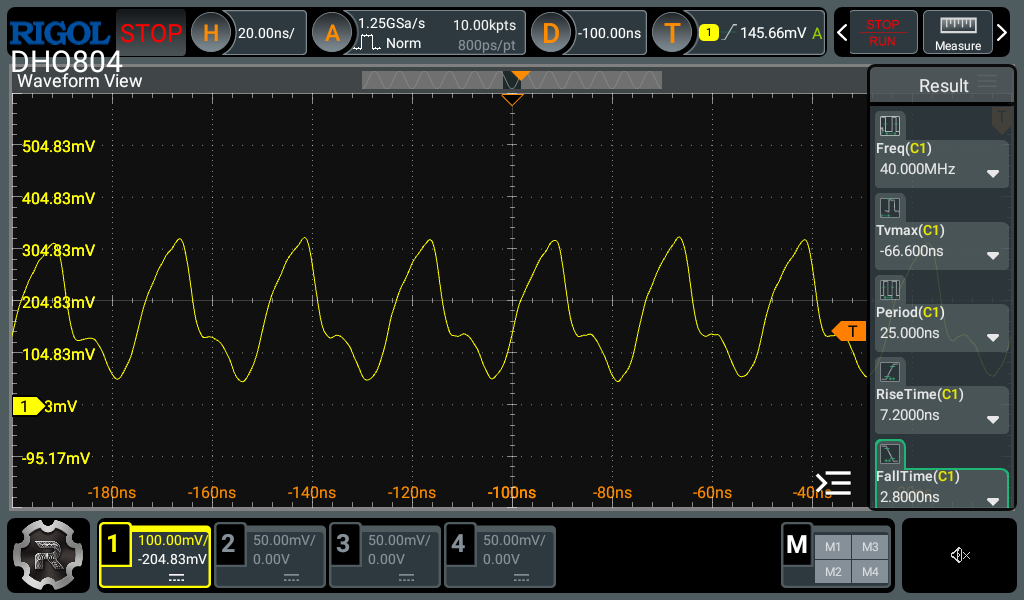
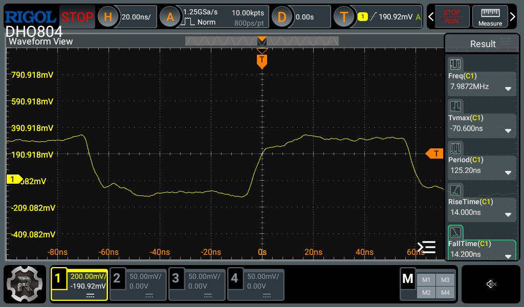
Pin 7 (CLKI) is the clock input. It's difficult to know if this is wrong, as there's no way to pause the system at each point in the startup process. Clocks may start off low (for compatibility reasons) before being set at whatever the board is configured for - if you have any knowledge in this area, let me know.
Faulty board (left) and Good board (right)
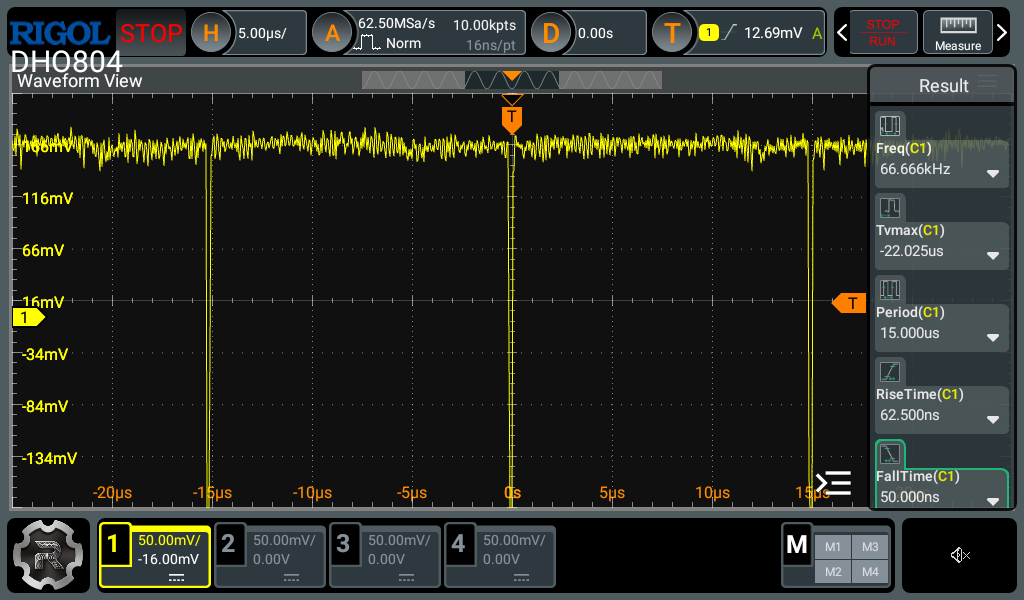
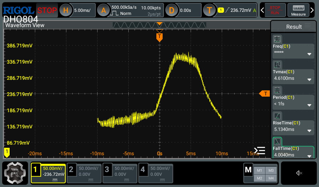
Pin 105 (OSC) is a 14.3 MHz oscillator input.
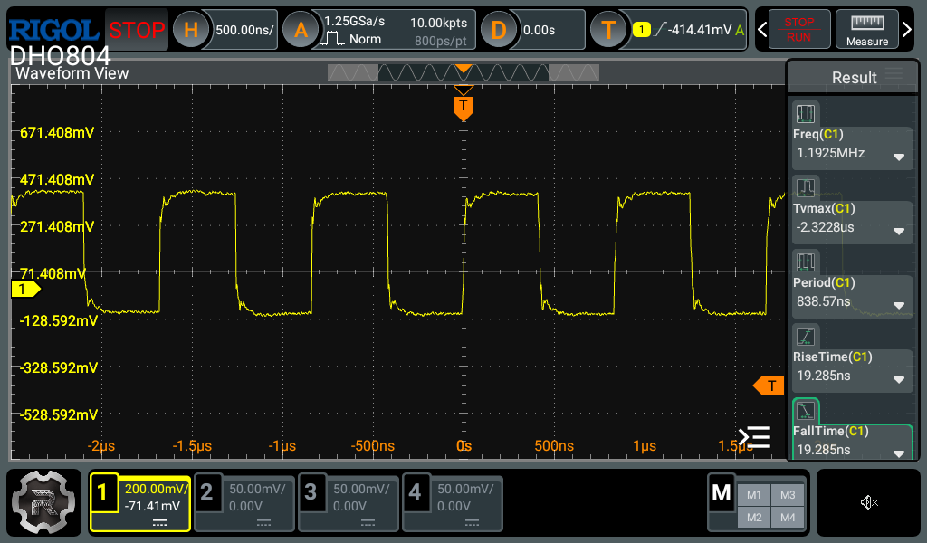
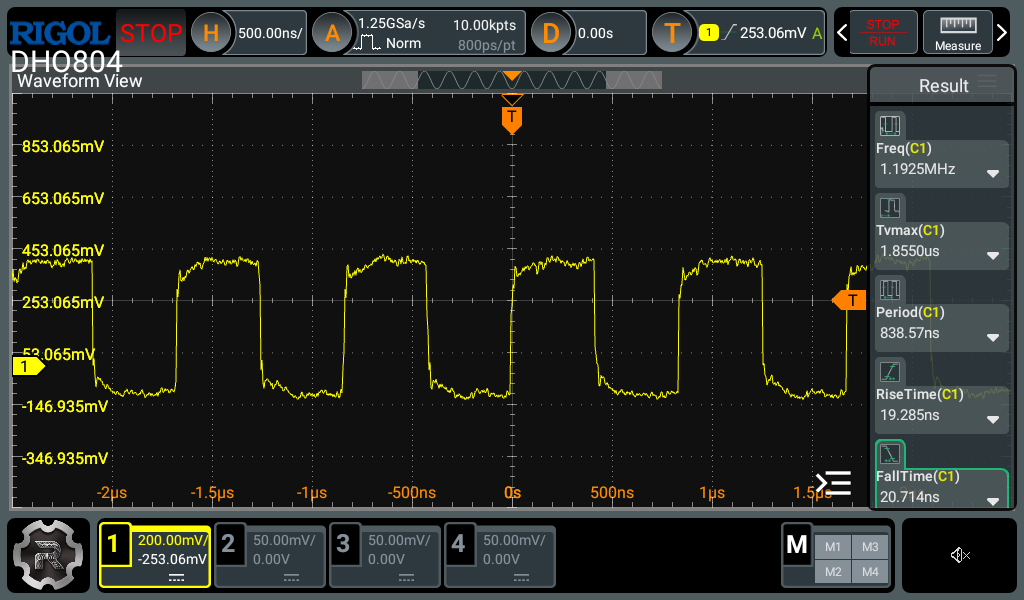
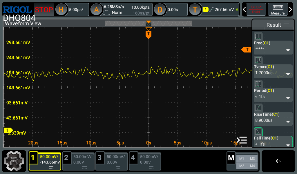
Pin 121 (OSC12) is a 1.19 MHz clock output to the 82C206, internally derived from OSC.
Faulty board (left) and Good board (right)
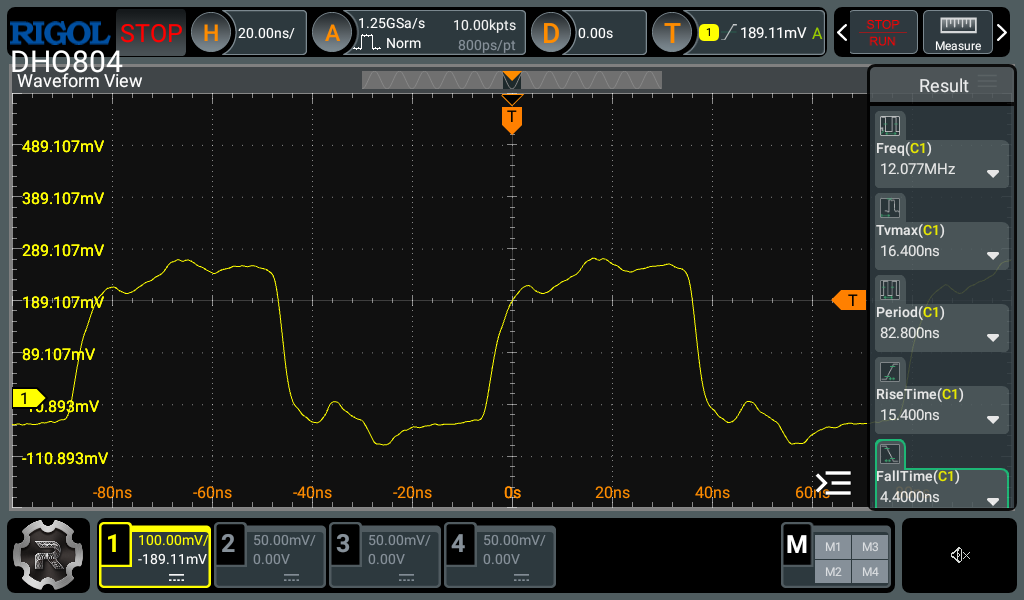
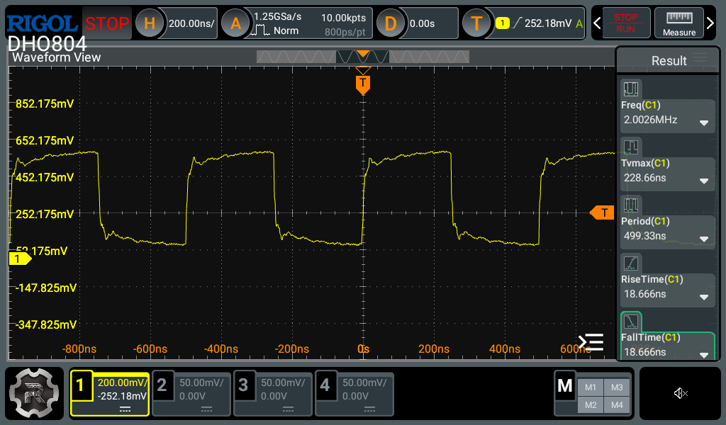
Pin 131 (ATCLK) is the output clock going to the AT bus. This could be CLKI/3, CLKI/4, CLKI/5 or CLKI/6. CLKI/6 is the default.
Faulty board (left) and Good board (right)
11) Is the Peripheral Controller bad?
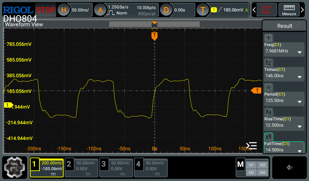
Pin 15 (SYSCLK) is the input clock signal (up to 10 MHz) - check to see if there is a clock signal coming in.
Faulty board (left) and Good board (right)
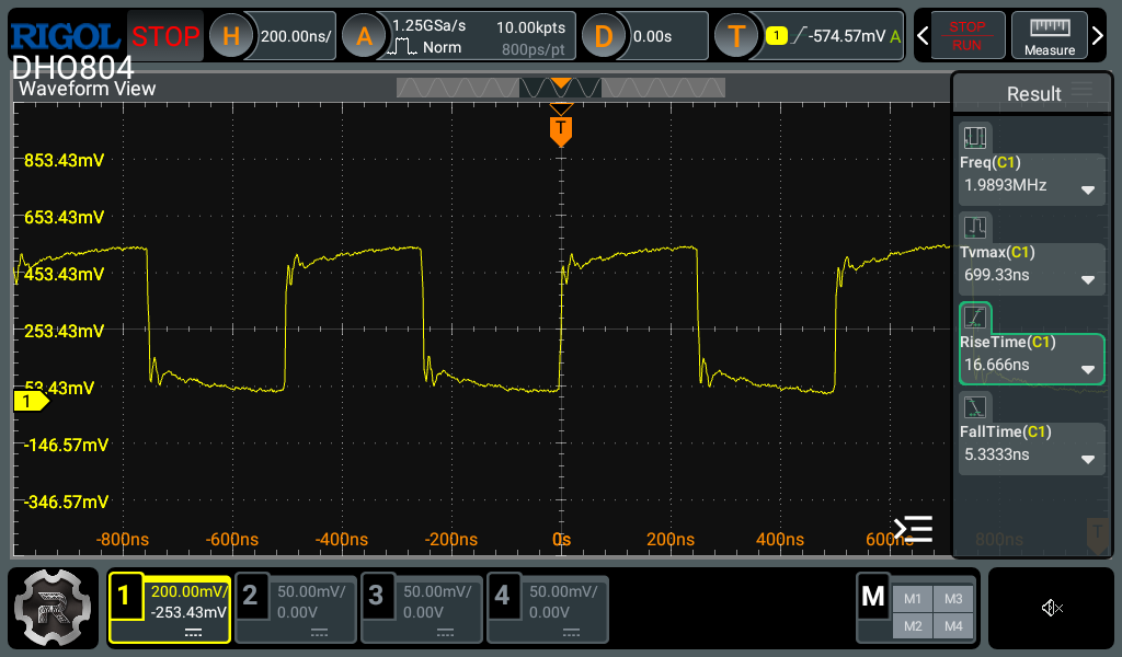
Pin 6 (PWRGD) is the 'power good' signal - this pin should be high when the PSU is on - if it's low, all address, data strobe, and read/write pins are disconnected from the CPU.
Faulty board (left) and Good board (right)
Also double-check the Vcc (pins 26 and 78) show an input voltage, and Vss (pins 3, 52 and 77) go to GND.
Pin 9 (TEST) should be tied low in normal operation.
Look out for Part 3 soon, where we'll continue troubleshooting with a look for CPU activity and then check out some of the TTL logic ICs.