Intel Chipsets
420EX - Aries
Award BIOS Chipset code: 2A499
This chipset is also referred to as the "Intel Green PC 82420EX PCIset".
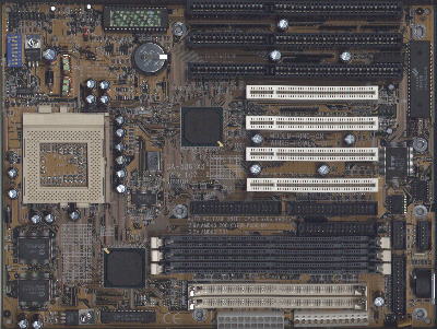
These motherboards used this chipset:
420TX - Saturn I / Saturn I EISA
Award BIOS Chipset codes: 2A496 (ISA) or 2B496 (EISA)
420ZX - Saturn II
Supports write-back level 1 cache. It does not support 40 MHz bus speed. Early suggestions were that this board would perform better than the SiS 496/497 and the VIA 82C486A/82C505 chipsets, but in reality it was slower than both.
These motherboards used this chipset:
ASUS PCI-I 486SP3G
Award BIOS Chipset Code: 2A498.
430EX AGPset
Supports 66 MHz front side bus.
430LX - Mercury (1993)
The first Pentium chipset released in 1993 for 60 and 66 MHz models. Supports PCI and FPM memory. These Pentiums were 5V chips and were used on the old socket 4 motherboards; they were rendered obsolete very quickly when Intel moved to their newer 90 and 100 MHz 3.3V processors running on socket 5 motherboards.
Feature-wise, the 430LX was a very plain chipset by today's standards. It included the PCI bus of course and support for up to 128 MB of RAM. There was no support for EDO memory (which was introduced in the Triton series). Cache chips were soldered directly onto most motherboards, and I believe the size was 64 KB. The 430LX went the way of the dodo very quickly, as did the motherboards it used and the hot, slow first-generation Pentiums they supported. Today it is extremely difficult to even find any information at all about this chipset!
Supports 66 MHz front side bus.
Award BIOS Chipset Codes: 2A597 or 2B597 or 2A59B
430NX - Neptune (1994)
The 430NX was the original chipset used for Intel's second generation Pentium chips, covering Pentiums with speeds from 90 to 133 MHz (which, of course, also work in later Pentium chipsets). The biggest improvement with this generation of technology was the newer Pentium itself: it ran much faster, cooler and more reliably than the first generation Pentiums did. In addition, the chipset itself introduced the following improvements over the Mercury (430LX) chipset:
- Dual processor support.
- Support for 512 MB of system memory (up from 128 MB for the Mercury).
- Support for up to 512 KB of asynchronous secondary cache.
While this was a good chipset, it didn't really introduce any major, ground-breaking new technologies, and it wasn't really well-publicized. Like the Mercury before it, it faded before the introduction of the Triton line, and about the only place to find information about it today is checking the motherboard manufacturers for spec sheets on their older boards.
Award BIOS Chipset Code: 2B59A
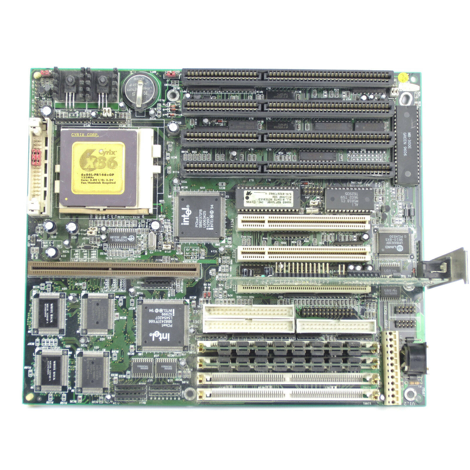
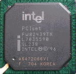
430FX - Triton (1995)
Intel made the first major jump into the chipset industry with the release of their very successful 430FX chipset, commonly known as the Intel Triton I or simply the FX Chipset.
Although now impractical for most applications, the 430FX was a very strong performer and competitor during its time. Most of the original Triton's success came courtesy of its memory and disk controllers. The 430FX was the very first Intel chipset designed to officially support the, at the time, newest memory standard, Extended Data Out Dynamic Random Access Memory (EDO DRAM for short) as well as pipeline burst SRAMs. This gave users, for the first time, the chance to get a taste of the high end market without shelling out the big bucks. The combination of high speed EDO DRAM with the advanced architectural features the original Pentium [Classic] had to offer made the FX Chipset ideal for most users, and that reign continued for quite some time as there was no real demand to replace the 430FX.
The Triton I also introduced the idea of using a technique called Busmastering to the enhanced IDE controller, which is the part of the chipset used for controlling EIDE peripherals (i.e. hard disks). These Busmastering capabilities were provided by the PIIX controller which in theory, and in practice, speeds up hard disk data transfers on either EIDE channel by granting EIDE peripherals certain SCSI like qualities. In spite of its strengths in memory support and hard disk access, the original Triton chipset had quite a few shortcomings. Although the 430FX allowed the use of up to 512KB of secondary Level 2 Pipeline Burst Cache (PBSRAM) and 128MB of RAM the chipset itself fails to cache any memory beyond the first 64MB. This posed a major problem to high end users expecting the maximum performance and power out of their systems.
The advantages of the 430FX over the 430NX are:
- Support for EDO memory.
- Supported for pipelined burst cache and synchronous cache technologies.
- PCI level 2.0 compliance.
- Improved performance, in general.
The disadvantages of the 430FX compared to the 430NX are:
- Less memory support (only 128 MB total).
- No support for dual processing.
Being the first member of the Triton family of chipsets the 430FX does not natively support any enhanced video features or caching schemes, the first introduction of such features came almost 2 years later with the release of the Intel 430VX chipset and its support for the Unified Memory Architecture. Power saving also isn't much of a strongpoint of the 430FX chipset, it fully supports the bare minimum requirements to be used in an "energy efficient" system, however features like Instant-On, and Suspend to Disk aren't included in this category. The performance of the original Triton isn't all that bad, however it is quite pointless to build a 430FX based system now since the torch has already been passed to the better designed 430HX and 430TX chipsets.
| Intel 82430FX Chipset | ||
| Common Name | Triton I | |
| Chipset Packaging | Number of chips | 3 (82437FX, 82438FX, 82371FB) |
| Packaging Type | 1 x 208-pin QFP; 2 x 100-pin QFP | |
| CPU Support | Number of CPUs | 1 |
| AMD CPUs Supported | N/A | |
| Cyrix CPUs Supported | N/A | |
| Intel CPUs Supported | Pentium | |
| Cache | Type | Asynchronous/Synchronous Pipeline Burst Cache |
| Maximum Supported Size | 512KB | |
| Maximum Cacheable DRAM Area | 64MB | |
| Memory | Maximum DRAM Supported | 128MB |
| BEDO DRAM Read Timings (66MHz) | N/A | |
| EDO DRAM Read Timings (66MHz) | 7-2-2-2 | |
| FPM DRAM Read Timings (66MHz) | 7-3-3-3 | |
| SDRAM Read Timings (66MHz) | N/A | |
| Data Path to Memory | 64-bits | |
| ECC Support | No | |
| Hard Disk Controller | Chip | PIIX (82371FB Controller) |
| Busmastering Support | Yes | |
| UltraDMA Support | No | |
| Max. Theoretical Transfer Rate | PIO Mode 4/DMA Mode 2 (16.6MB/S) | |
| PCI Interface | Supported PCI Bus Speeds | 25, 30, 33 MHz |
| Concurrent PCI | No | |
| Async. PCI Bus Speed | No | |
| PCI Specification | 2.0 (66 MHz max.) | |
| Power Management | PC97 Compliance | No |
| Suspend to Disk | No | |
| HDD Power Down | Yes | |
| Modem Wakeup | No | |
| System Suspend | No | |
| Video | AGP Support | No |
| Unified Memory Architecture | No | |
| Peripheral Support | USB Support | No |
| Plug and Play Port | Yes | |
| Write Buffers | CPU-to-DRAM | 4 QWords |
| CPU-to-PCI | 4 DWords | |
| PCI-to-DRAM | 12 DWords | |
| Officially Supported Bus Speeds | 50, 60, 66 MHz | |
| Unofficially Achieved Bus Speeds | None | |
Award BIOS Chipset code: 2A59C
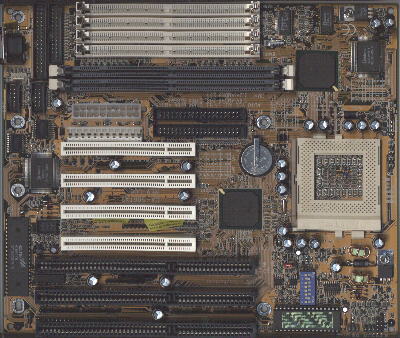
Motherboards that use this chipset are:
- Microstar MS-5120
- BioStar MB-8500TAC
- Elpina M507
- Soyo SY-5TE2 and ST-5TE5
- Octek Rhino-6
430MX (1995)
The 430MX chipset is a version of the Intel 430FX chipset designed for portable computers.
| Intel 82430MX Chipset | ||
| Common Name | - | |
| Chipset Packaging | Number of chips | 3 (82437MX, 82438MX, 82371MX) |
| Packaging Type | 1 x 208-pin QFP; 1 x 100-pin TQFP | |
| CPU Support | Number of CPUs | 1 |
| AMD CPUs Supported | N/A | |
| Cyrix CPUs Supported | N/A | |
| Intel CPUs Supported | Pentium 75, 90, 120 | |
| Cache | Type | Asynchronous/Synchronous Pipeline Burst Cache |
| Maximum Supported Size | 512KB | |
| Maximum Cacheable DRAM Area | 64MB | |
| Memory | Maximum DRAM Supported | 128MB |
| BEDO DRAM Read Timings (66MHz) | N/A | |
| EDO DRAM Read Timings (66MHz) | 7-2-2-2 | |
| FPM DRAM Read Timings (66MHz) | 7-3-3-3 | |
| SDRAM Read Timings (66MHz) | N/A | |
| Data Path to Memory | 64-bits | |
| ECC Support | No | |
| Hard Disk Controller | Chip | MPIIX (82371MX Controller) |
| Busmastering Support | Yes | |
| UltraDMA Support | No | |
| Max. Theoretical Transfer Rate | PIO Mode 4/DMA Mode 2 (16.6MB/S) | |
| PCI Interface | Supported PCI Bus Speeds | 25, 30, 33 MHz |
| Concurrent PCI | No | |
| Async. PCI Bus Speed | No | |
| PCI Specification | 2.0 (66 MHz max.) | |
| Power Management | PC97 Compliance | No |
| Suspend to Disk | No | |
| HDD Power Down | Yes | |
| Modem Wakeup | No | |
| System Suspend | No | |
| Video | AGP Support | No |
| Unified Memory Architecture | No | |
| Peripheral Support | USB Support | No |
| Plug and Play Port | Yes | |
| Write Buffers | CPU-to-DRAM | 4 QWords |
| CPU-to-PCI | 4 DWords | |
| PCI-to-DRAM | 12 DWords | |
| Officially Supported Bus Speeds | 50, 60, 66 MHz | |
| Unofficially Achieved Bus Speeds | None | |
430HX - Triton II (1996)
With Intel's newly found place in the chipset industry they decided to improve on their already outstanding design by creating the long awaited successor to the 430FX chipset. This time around, Intel focused their attention more on high end speed and power rather than simply "getting the job done". It is this attitude that gave the 430HX chipset the leading edge over the rest of the market for quite some time, however motherboard manufacturers were reluctant to charge the outstanding cost of the HX chipset. Some manufacturers decided to cut corners by including a degraded Tag RAM chip which only enables the first 64MB of RAM to be cached instead of the Maximum 512MB.
The HX chipset's primary advantages over the FX are:
- Support for parity and ECC memory.
- Dual processor support.
- Support for 512 MB of system memory instead of just 128 MB.
- Support for 512 MB of cached system memory instead of just 64 MB (if the optional larger tag RAM is installed.)
- Much improved performance, due to faster memory timing and more I/O buffers.
- PCI level 2.1 compliance.
- USB support.
- Independent device timing for IDE/ATA drives.
This is a full-featured chipset, and has been the most popular Intel Pentium chipset for those who are performance-oriented. Motherboards using it tend to be slightly more expensive than those using the FX or VX chipsets. Its biggest advantages are its faster performance, much larger maximum cacheable RAM, and parity / error correction support.
The Performance of the Triton II is still quite competitive today with most higher end processors and configurations. Unlike the original triton, this successor has the ability to support dual CPUs as well as ECC DRAM and USB. The EDO timings on the HX Chipset are considerably faster than those on the FX chipset which means you can expect a greater overall memory performance with the HX Chipset, especially if using over 64MB of RAM, the cacheable limit of the FX. The HX Chipset also extends CPU compatibility to IBM/Cyrix as well as AMD and Intel which makes it a better competitor even today. Its PIIX3 BMIDE Controller is considerably faster than the PIIX controller found in the FX chipset, however it still doesn't support the UltraDMA specification. The Triton II was also the first chipset to even unofficially support the 83.3MHz bus frequency now very common in most decent motherboards today.
| Common Name | Triton II | |
| Chipset Packaging | Number of chips | 2 (82439HX System Controller, 82371SB) |
| Packaging Type | 1 x 324-pin BGA; 1 x 208-pin lead QFP | |
| CPU Support | Number of CPUs | 2 |
| AMD CPUs Supported | K5, K6 | |
| Cyrix CPUs Supported | 6x86 (M1), 6x86MX (M2) | |
| Intel CPUs Supported | Pentium, Pentium MMX | |
| Cache | Type | Pipeline Burst Cache |
| Maximum Supported Size | 512KB | |
| Maximum Cacheable DRAM Area | 64MB or 512MB (depending on Tag RAM) | |
| Memory | Maximum DRAM Supported | 512MB |
| BEDO DRAM Read Timings (66MHz) | N/A | |
| EDO DRAM Read Timings (66MHz) | 5-2-2-2 | |
| FPM DRAM Read Timings (66MHz) | 5-3-3-3 | |
| SDRAM Read Timings (66MHz) | N/A | |
| Data Path to Memory | 64-bits | |
| ECC Support | Yes | |
| Hard Disk Controller | Chip | PIIX3 (82371SB Controller) |
| Busmastering Support | Yes | |
| UltraDMA Support | No | |
| Max. Theoretical Transfer Rate | PIO Mode 4/DMA Mode 2 (16.6MB/S) | |
| PCI Interface | Supported PCI Bus Speeds | 25, 30, 33 MHz |
| Concurrent PCI | Yes | |
| Async. PCI Bus Speed | No | |
| PCI Specification | 2.0 (66 MHz max.) | |
| Power Management | PC97 Compliance | No |
| Suspend to Disk | No | |
| HDD Power Down | Yes | |
| Modem Wakeup | No | |
| System Suspend | No | |
| Video | AGP Support | No |
| Unified Memory Architecture | No | |
| Peripheral Support | USB Support | Yes |
| Plug and Play Port | Yes | |
| Write Buffers | CPU-to-DRAM | 16 QWords |
| CPU-to-PCI | 6 DWords | |
| PCI-to-DRAM | 20 DWords | |
| Officially Supported Bus Speeds | 50, 55, 60, 66 MHz | |
| Unofficially Achieved Bus Speeds | 68, 75, 83.3 MHz | |
Award BIOS Chipset Codes: 2A59F or 2B59F
AwardBIOS CMOS Setup Utility User's Guide for Intel 82430HX PCIset (EliteBIOS v4.51PG) - for BIOS Part #2A59Fxxx
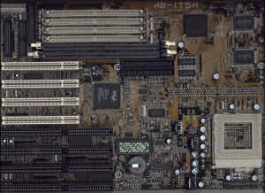
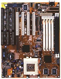
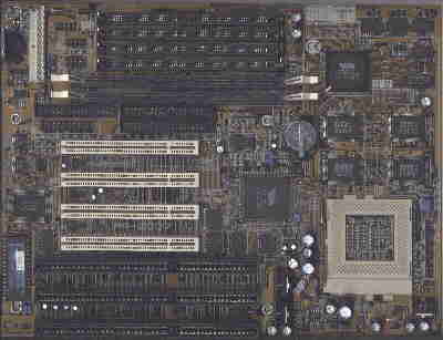
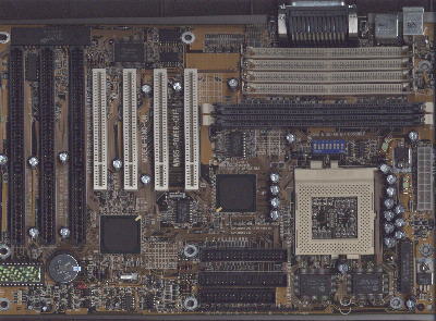
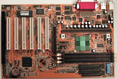
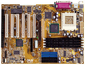
Motherboards that use the 430HX chipset are:
- AsusTek P/I P65 UP5 (Socket 7, AT)
- ABit AB-IT5H (Socket 7, AT)
- Gigabyte GA-586 HX2 (Socket 7, AT)
- Shuttle HOT-553 (Socket 7, AT)
- Tyan S1564D 'Tomcat IV' (Socket 7, Baby AT)
- Octek Rhino-9
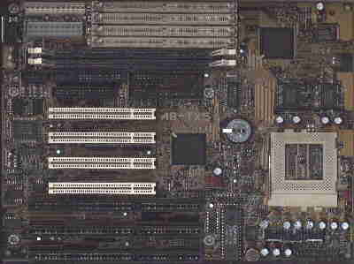
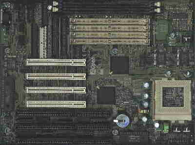
430TX (1997)
 Intel, now currently embedded in the Chipset Industry, decided to make another giant leap with the final addition to the Socket-7 line of chipsets, originally thought of as being called the Triton IV chipset and boasting features not even found in the HX chipset the TX chipset turned out to be a bit of a disappointment for most users, although not all.
The TX Chipset was intended to be the first and last Socket-7 chipset to be able to boast high end features such as SDRAM and USB support while allowing the user a variety of power saving options to use. The highly integrated 2 chip packaging solution found in the TX chipset is superior even to that of the 430HX chipset, one of the few areas in which the TX chipset is actually superior to the HX. The SDRAM performance of the TX chipset isn't "bone shattering" due to a timing problem with the chipset (which has been corrected in the Pentium II successor to the TX chipset, the LX chipset), however the stability of SDRAM and the TX chipset at higher bus speeds is much greater than that of EDO and the HX Chipset.
The UltraDMA specification is another plus of the TX chipset, with theoretical transfer rates as high as 33MB/S, nearly equivalent to UltraWide SCSI-3 performance although that number cannot be reproduced significantly in real world applications. Unfortunately the TX chipset still doesn't have the deep CPU and PCI buffers found in the HX chipset, however the performance difference between the TX and the HX chipsets is barely noticeable. The 256MB maximum memory limit of the TX chipset is blurred by its meager 64MB cacheable memory area which takes us back to the old days of the FX chipset. Intel made the TX chipset the proper fare well to the Socket-7 standard in order to make way for the new Slot-1 motherboards, however what they failed to realize was that by not giving the user the option of AGP in a Socket-7 motherboard other companies such as VIA are able to step up and satisfy this need and many more..
| Common Name | Triton TX | |
| Chipset Packaging | Number of chips | 2 ((82439TX System Controller, 82371AB) |
| Packaging Type | 2 x 324-pin BGA | |
| CPU Support | Number of CPUs | 1 |
| AMD CPUs Supported | K5, K6 | |
| Cyrix CPUs Supported | 6x86 (M1), 6x86MX (M2) | |
| Intel CPUs Supported | Pentium, Pentium MMX | |
| Cache | Type | Pipeline Burst Cache |
| Maximum Supported Size | 512KB | |
| Maximum Cacheable DRAM Area | 64MB | |
| Memory | Maximum DRAM Supported | 256MB |
| BEDO DRAM Read Timings (66MHz) | N/A | |
| EDO DRAM Read Timings (66MHz) | 5-2-2-2 | |
| FPM DRAM Read Timings (66MHz) | 5-3-3-3 | |
| SDRAM Read Timings (66MHz) | 5-1-1-1 | |
| Data Path to Memory | 64-bits | |
| ECC Support | No | |
| Hard Disk Controller | Chip | PIIX4 (82371AB Controller) |
| Busmastering Support | Yes | |
| UltraDMA Support | Yes | |
| Max. Theoretical Transfer Rate | PIO Mode 5/DMA Mode 3 (33.3MB/S) | |
| PCI Interface | Supported PCI Bus Speeds | 25, 30, 33 MHz |
| Async. PCI Bus Speed | No | |
| PCI Specification | 2.0 (66 MHz max.) | |
| Power Management | PC97 Compliance | Yes |
| Suspend to Disk | Yes | |
| HDD Power Down | Yes | |
| Modem Wakeup | Yes | |
| System Suspend | Yes | |
| Video | AGP Support | No |
| Unified Memory Architecture | No | |
| Peripheral Support | USB Support | Yes |
| Plug and Play Port | Yes | |
| Write Buffers | CPU-to-DRAM | 16 QWords |
| CPU-to-PCI | 6 DWords | |
| PCI-to-DRAM | 18 DWords | |
| Officially Supported Bus Speeds | 50, 55, 60, 66 MHz | |
| Unofficially Achieved Bus Speeds | 68, 75, 83.3 MHz | |
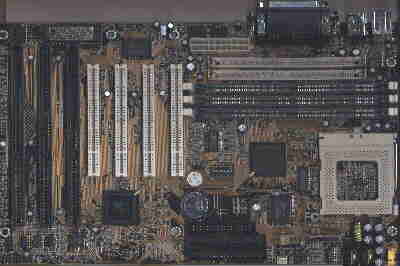
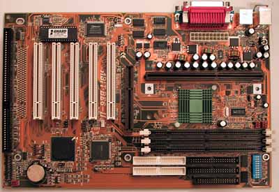
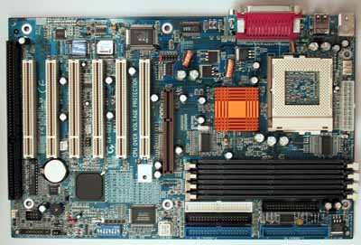
Motherboards that use this chipset are:
ABit AB-AX5 - Socket 7, ATX
ABit AB-PX5 - Socket 7, AT
ABit AB-TX5 - Socket 7, AT
AOpen AP5T - Socket 7, AT
AOpen AX5T - Socket 7, ATX
AsusTek P/I P55 TXP4 - Socket 7, AT
AsusTek TX97-E - Socket 7, AT
AsusTek TX97-XE - Socket 7, ATX
FIC PA-2007 - Socket 7, AT
Chaintech 5TDM2 - Socket 7, AT
Gigabyte GA-586TX3 - Socket 7, AT
Gigabyte GA-586TX2 - Socket 7, AT
Gigabyte GA-586ATX03 - Socket 7, ATX
Lucky Star 5I-TX2A - Socket 7, ATX
Octek Rhino-15 / Rhino-15+
Octek Rhino-20 / Rhino-20+
Shuttle HOT-565 - Socket 7, AT
Shuttle HOT-569 - Socket 7, AT
Soyo 5XA5 - Socket 7, ATX
Tyan S1571 'Titan Turbo' - Socket 7, Baby AT
Award BIOS Chipset code: 2A59I
AwardBIOS CMOS Setup Utility User's Guide for Intel 82430TX PCIset (EliteBIOS v4.51PG) - for BIOS Part #2A59Ixxx
430VX - Triton III / Triton VX (1996)
 By this time, Intel had two titles under their belt with the success of the FX and HX chipsets, however something was missing. The market demanded a chipset to fill the void between the original FX chipset and the much more powerful and more expensive HX chipset. What was to be used in desktop computers for the home or low cost situations?
Answering this cry for help Intel released the VX chipset, commonly referred to as the Triton III which can be quite misleading since it is in no way superior to the Triton II when it comes to performance. The 430VX is plagued by the 64MB cacheable memory limit as well as poor performance as a direct cause of a lack of CPU-to-PCI buffers, something unheard of in the 430HX Chipset. However Intel made up for this by equipping the VX chipset with the ability to support SDRAM, a newer, faster type of DRAM as well as adding support for the Unified Memory Architecture, UMA for short. UMA can be thought of as a sort of pre-AGP which allows your video card to share your system memory with the sacrifice of some performance, about a 5% loss overall. Unfortunately with SDRAM and UMA support the 430VX still cannot compete head to head with the HX chipset nor VIA's line of Apollo chipsets, however it still provides excellent performance for the price.
The VX chipset's advantages over the HX:
- Lower cost.
- Support for SDRAM.
- Improved burst memory reads when using SDRAM (though the initial read is slower). The timing with SDRAM is 7-1-1-1 vs. the HX's 5-2-2-2 when using EDO RAM.
The VX chipset's disadvantages compared to HX:
- No parity or ECC memory support.
- No dual processor support.
- Support for only 128 MB of system memory, like the FX.
- Support for only 64 MB of cached system memory, again, like the FX.
- Slower memory timings when using EDO memory (but faster than the FX).
- Fewer PCI I/O buffers (but more than the FX).
- No independent device timing for IDE/ATA devices.
- Fewer supported motherboard SIMM or DIMM slots.
The advantage of SDRAM over EDO RAM in Pentium systems is questionable; while the raw speed of SDRAM is much higher than EDO, only 5 to 10 percent of requests for memory reads actually go to the memory. The vast majority are satisfied by the level 2 cache; the end result is that SDRAM does not lead to nearly as large an increase in performance as its presence might imply.
| Common Name | Triton III | |
| Chipset Packaging | Number of chips | 3 (82437VX System Controller, 82438VX, 82371SB) |
| Packaging Type | 2 x 208-pin lead QFP; 1 x 100-pin lead QFP | |
| CPU Support | Number of CPUs | 1 |
| AMD CPUs Supported | K5, K6 | |
| Cyrix CPUs Supported | 6x86 (M1), 6x86MX (M2) | |
| Intel CPUs Supported | Pentium, Pentium MMX | |
| Cache | Type | Pipeline Burst Cache |
| Maximum Supported Size | 512KB | |
| Maximum Cacheable DRAM Area | 64MB | |
| Memory | Maximum DRAM Supported | 128MB |
| BEDO DRAM Read Timings (66MHz) | N/A | |
| EDO DRAM Read Timings (66MHz) | 6-2-2-2 | |
| FPM DRAM Read Timings (66MHz) | 6-3-3-3 | |
| SDRAM Read Timings (66MHz) | 7-1-1-1 | |
| Data Path to Memory | 64-bits | |
| ECC Support | No | |
| Hard Disk Controller | Chip | PIIX3 (82371SB Controller) |
| Busmastering Support | Yes | |
| UltraDMA Support | No | |
| Max. Theoretical Transfer Rate | PIO Mode 4/DMA Mode 2 (16.6MB/S) | |
| PCI Interface | Supported PCI Bus Speeds | 25, 30, 33 MHz |
| Concurrent PCI | Yes | |
| Async. PCI Bus Speed | No | |
| PCI Specification | 2.0 (66 MHz max.) | |
| Power Management | PC97 Compliance | No |
| Suspend to Disk | No | |
| HDD Power Down | Yes | |
| Modem Wakeup | No | |
| System Suspend | No | |
| Video | AGP Support | No |
| Unified Memory Architecture | Yes | |
| Peripheral Support | USB Support | Yes |
| Plug and Play Port | Yes | |
| Write Buffers | CPU-to-DRAM | 16 QWords |
| CPU-to-PCI | 5 DWords | |
| PCI-to-DRAM | 18 DWords | |
| Officially Supported Bus Speeds | 50, 55, 60, 66 MHz | |
| Unofficially Achieved Bus Speeds | 68, 75, 83.3 MHz | |
Award BIOS Chipset code: 2A59G or 2A59H (illegal BIOS)
AwardBIOS CMOS Setup Utility User's Guide for Intel 82430VX PCIset (EliteBIOS v4.51PG) - for BIOS Part #2A59Gxxx
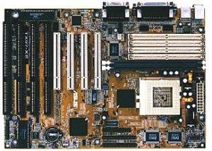
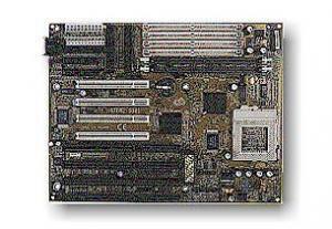
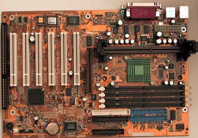
Motherboards that use this chipset are:
- ABit AB-AR5
- ABit AB-SM5
- BioStar MB-8500TVX-A
- Chaintech 5IFM
- Elitegroup ECS-P5VX-A
- Gigabyte GA-586VX
- Gigabyte GA-586ATV
- Mercury W586 VXL - Socket 7, AT
- Octek Rhino-6VX
- Octek Rhino-10
- Soyo SY-5VA / SY-5VA2
- Soyo SY-5VD
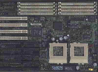
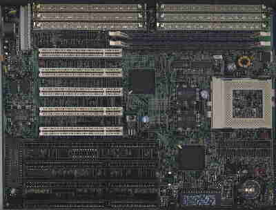
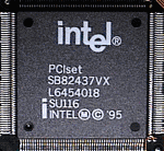
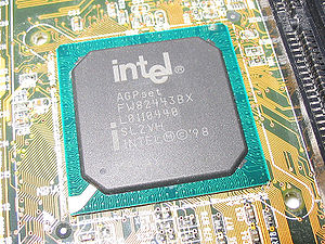
440FX - 82440FX Natoma (1997?)
Intel had already taken care of the Pentium market, or so they believed, with the Triton series of chipsets, however how were they supposed to support their expensive "new" creation, the Pentium Pro (and now the Pentium II)? The 440FX Chipset, commonly known as the Natoma Chipset, was designed to be a real monster of a chipset, to be the strong base for a powerful Pentium Pro/II based system.
Unlike previous chipsets, the 440FX didn't have the problem of a cacheable memory area being limited, since the Pentium Pro's internal L2 cache and the Pentium II's on-card L2 cache takes care of all RAM caching, instead of the chipset. With that bottleneck taken care of, the 440FX already appears to be an excellent reason to upgrade from a Socket-7 CPU. However it does lack features such as support for SDRAM and APM (Advanced Power Management) but it compensates by adding support for BEDO DRAM and lower CPU utilization for simple operations.
To fit its server role, the Natoma Chipset allows a maximum of 2 processors to be used using the Symmetric Multiprocessing standalone I/O APIC component, a 64-pin lead QFP chip. The 440FX chipset also continues to make excellent use of Intel's Concurrent PCI Architecture which allows for lower CPU utilization when performing operations which take advantage of the integrated multi-transaction timer such as video playback. Like the 430VX and HX chipsets, the Natoma uses the PIIX3 Busmastering EIDE controller to ensure backwards compatibility with all previously released products.
| Common Name | Natoma | |
| Chipset Packaging | Number of chips | 3 (82441FX PMC, 82442FX DBX, 82371SB) 1 (optional - 82093AA for SMP) |
| Packaging Type | 3 x 208-pin QFP 1 x 64-pin lead QFP (optional) |
|
| CPU Support | Number of CPUs | 2 (SMP) |
| AMD CPUs Supported | N/A | |
| Cyrix CPUs Supported | N/A | |
| Intel CPUs Supported | Pentium Pro, Pentium II | |
| Cache | Type | N/A on chip |
| Maximum Supported Size | N/A on chip | |
| Maximum Cacheable DRAM Area | N/A on chip | |
| Memory | Maximum DRAM Supported | 1024MB |
| BEDO DRAM Read Timings (66MHz) | 5-1-1-1 | |
| EDO DRAM Read Timings (66MHz) | 5-2-2-2 | |
| FPM DRAM Read Timings (66MHz) | 5-3-3-3 | |
| SDRAM Read Timings (66MHz) | N/A | |
| Data Path to Memory | 64-bits | |
| ECC Support | Yes | |
| Hard Disk Controller | Chip | PIIX3 (82371SB Controller) |
| Busmastering Support | Yes | |
| UltraDMA Support | No | |
| Max. Theoretical Transfer Rate | PIO Mode 4/DMA Mode 2 (16.6MB/S) | |
| PCI Interface | Supported PCI Bus Speeds | 30, 33 MHz |
| Async. PCI Bus Speed | No | |
| PCI Specification | 2.1 (66 MHz max.) | |
| Power Management | PC97 Compliance | Yes |
| Suspend to Disk | Yes | |
| HDD Power Down | Yes | |
| Modem Wakeup | Yes | |
| System Suspend | Yes | |
| Video | AGP Support | No |
| Unified Memory Architecture | No | |
| Peripheral Support | USB Support | Yes |
| Plug and Play Port | Yes | |
| Write Buffers | CPU-to-DRAM | 16 QWords |
| CPU-to-PCI | 6 DWords | |
| PCI-to-DRAM | 20 DWords | |
| Officially Supported Bus Speeds | 60, 66 MHz | |
| Unofficially Achieved Bus Speeds | 68, 75, 83.3 MHz | |
Award BIOS Chipset code: 2A69H
AwardBIOS CMOS Setup Utility User's Guide for Intel 82440FX PCIset (AwardBIOS v4.51PG) - for BIOS Part #2A69Hxxx
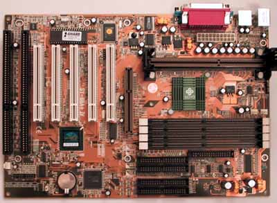
Motherboards that used the 440FX chipset include:
- Octek Rhino Pro 1
- Octek Rhino Pro 6
- Octek Rhino II
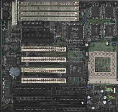
440LX / 82440LX - Balboa (1998?)
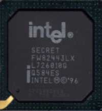 Intel announced back in June that they would be soon releasing their first AGPSet exclusively for the Pentium II, implying that they would be giving up on the Pentium MMX and Pentium Pro line of chipsets. Sure enough, when September came around Intel gave us an expected surprise with the release of the 440LX Chipset, a chipset combining the best of the 430TX and 440FX chipsets.
The result of months of hard work and testing was a chipset, supporting only the Pentium II, with official support for AGP, SDRAM, the UltraATA HDD specification, and full PC97 compliance. The deep buffers between DRAM and the CPU remain unmatched by any other Intel chipset, and like the 440FX the LX supports a maximum of Dual Processors. The single chip design of the 440LX chipset is something you don't see very much in the chipset industry, but something you will begin to see much more of especially with some upcoming products from VIA as well as future Intel chipsets.
The LX Chipset, being the first Pentium II chipset to support SDRAM, supports a maximum of 512MB of SDRAM and a whopping 1GB of EDO if you opt for the slower standard. Fortunately, the LX chipset is able to improve performance when SDRAM is used with it by requiring special modules with onboard EEPROM to be used to enable communications between the chipset and the RAM. However, older modules lacking this EEPROM still work with the chipset almost flawlessly.
| Common Name | LX AGPSet | |
| Chipset Packaging | Number of chips | 1 (82443LX) |
| Packaging Type | 1 x 492-pin BGA | |
| CPU Support | Number of CPUs | 2 (SMP) |
| AMD CPUs Supported | N/A | |
| Cyrix CPUs Supported | N/A | |
| Intel CPUs Supported | Pentium II | |
| Cache | Type | N/A on chip |
| Maximum Supported Size | N/A on chip | |
| Maximum Cacheable DRAM Area | N/A on chip | |
| Memory | Maximum DRAM Supported | 512MB (SDRAM); 1024MB (EDO) |
| BEDO DRAM Read Timings (66MHz) | N/A | |
| EDO DRAM Read Timings (66MHz) | 5-2-2-2 | |
| FPM DRAM Read Timings (66MHz) | N/A | |
| SDRAM Read Timings (66MHz) | 5-1-1-1 | |
| Data Path to Memory | 64-bits | |
| ECC Support | Yes | |
| Hard Disk Controller | Chip | PIIX4 (82371AB Controller) |
| Busmastering Support | Yes | |
| UltraDMA Support | Yes | |
| Max. Theoretical Transfer Rate | PIO Mode 5/DMA Mode 3 (33.3MB/S) | |
| PCI Interface | Supported PCI Bus Speeds | 30, 33 MHz |
| Async. PCI Bus Speed | No | |
| PCI Specification | 2.1 (66 MHz max.) | |
| Power Management | PC97 Compliance | Yes |
| Suspend to Disk | Yes | |
| HDD Power Down | Yes | |
| Modem Wakeup | Yes | |
| System Suspend | Yes | |
| Video | AGP Support | Yes (66/133) |
| Unified Memory Architecture | No | |
| Peripheral Support | USB Support | Yes |
| Plug and Play Port | Yes | |
| Write Buffers | CPU-to-DRAM | Unknown |
| CPU-to-PCI | Unknown | |
| PCI-to-DRAM | Unknown | |
| Officially Supported Bus Speeds | 60, 66 MHz | |
| Unofficially Achieved Bus Speeds | 68, 75, 83.3, ~100 MHz | |
Motherboards that used the 440LX chipset include:
- Octek Rhino LX
440BX - Seattle (1998)
 As you can tell by the below Specification chart the Intel BX chipset isn't all that different from the 440LX chipset. The real division between the two chipsets is the 440BX's official support for the 100MHz Bus Frequency, a 50% increase in the clock of the system bus from Intel's previous standard, the 66MHz bus.
Not only will this increased bus frequency bring us higher clock speeds, but it will also provide the users with increased memory performance due to the System memory operating at the 100MHz bus speed, in comparison to the conventional 66MHz setting.
| Common Name | BX AGPSet | |
| Chipset Packaging | Number of chips | 1 (82443BX) |
| Packaging Type | 1 x 492-pin BGA | |
| CPU Support | Number of CPUs | 2 (SMP) |
| AMD CPUs Supported | N/A | |
| Cyrix CPUs Supported | N/A | |
| Intel CPUs Supported | Pentium II | |
| Cache | Type | N/A on chip |
| Maximum Supported Size | N/A on chip | |
| Maximum Cacheable DRAM Area | N/A on chip | |
| Memory | Maximum DRAM Supported | 512MB (SDRAM); 1024MB (EDO) |
| BEDO DRAM Read Timings (66MHz) | N/A | |
| EDO DRAM Read Timings (66MHz) | 5-2-2-2 | |
| FPM DRAM Read Timings (66MHz) | N/A | |
| SDRAM Read Timings (66MHz) | 5-1-1-1 | |
| Data Path to Memory | 64-bits | |
| ECC Support | Yes | |
| Hard Disk Controller | Chip | PIIX4 (82371AB Controller) |
| Busmastering Support | Yes | |
| UltraDMA Support | Yes | |
| Max. Theoretical Transfer Rate | PIO Mode 5/DMA Mode 3 (33.3MB/S) | |
| PCI Interface | Supported PCI Bus Speeds | 30, 33 MHz |
| Async. PCI Bus Speed | No | |
| PCI Specification | 2.1 (66 MHz max.) | |
| Power Management | PC97 Compliance | Yes |
| Suspend to Disk | Yes | |
| HDD Power Down | Yes | |
| Modem Wakeup | Yes | |
| System Suspend | Yes | |
| Video | AGP Support | Yes (66/133) |
| Unified Memory Architecture | No | |
| Peripheral Support | USB Support | Yes |
| Plug and Play Port | Yes | |
| Officially Supported Bus Speeds | 66, 100 MHz | |
| Unofficially Achieved Bus Speeds | 75, 83, 103, 112, 133 MHz | |
Award BIOS Chipset Code: 3A69K (same for 440ZX) or 2A69K
AwardBIOS CMOS Setup Utility User's Guide for Intel 82440BX AGPset (AwardBIOS v4.51PG) - for BIOS Part #2A69Kxxx
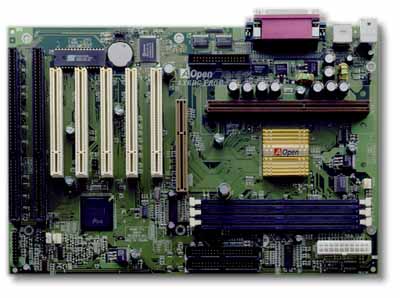
Motherboards that use this chipset are:
Abit BF6 - Slot 1, ATX
ABit BE6-II - Slot 1, ATX
AOpen AX6BC Pro Gold - Slot 1, ATX
ASUS CUBX - Socket 370, ATX
Gigabyte GA-6BX7 - Socket 370, ATX
Microstar BXMaster - Slot 1, ATX
Soyo SY-6BA+IV - Slot 1, ATX
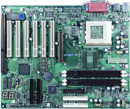
EPOX EP-BX7+ - Slot 370, ATX
440ZX (1998)
 The 440ZX was based on the successful 440BX Seattle chipset, but was designed for the lower cost "entry-level" PC market, typically running on a micro-ATX form factor.
Since 440BX supported 2xAGP for the first time, it was important that 440ZX also provided this same functionality.
440GX - 82440GX
The 440BX chipset from Intel was thought to be the killer in the Slot-1 world, however limitations the chipset provided would keep it away from the high end workstation and server markets. While a 512MB memory capacity is plenty for most users, a high end server can easily find good use for that much and beyond, therefore presenting the need for a new chipset: the Intel 440GX AGPSet. Pretty much everything the 440BX should have been, with support for a new processor, the 440GX is Intel's latest AGPSet designed to tailor to the high end market instead of the home user.
All work and no play would make any high end workstation a bore, which is why Intel left in all of the key features the 440BX chipset brought to the table when they designed the GX AGPSet. The AGP 2X specification is completely provided for by the GX, including multi-processor support for up to 2 CPU's. The GX begins to differ from its older brother here, in its processor support. While supporting the standard, run-of-the-mill Pentium II processors the 440GX also supports Intel's newest concoction, the Slot-2 based Xeon processor. Mainly geared towards server markets, and possibly high end workstation platforms, the Intel Xeon will find its home quite comfortable on a 440GX based motherboard. The GX, as mentioned before, features all of the benefits the 440BX brought to the industry, including support for the 100MHz Front Side Bus frequency and SDRAM while expanding on the BX design to include for memory configurations of up to 2GB of SDRAM.
Completely removing support for older memory types such as EDO DRAM, which was previously supported in the BX and LX chipsets, the 440GX AGPSet is a solution for only the most power hungry and performance crazed users. At the same time the 440GX can make for an affordable companion to a Xeon processor without sacrificing any of the fun components such as AGP video cards and other such things that we would normally be without if a different chipset were to be chosen (i.e. the other chipset from Intel with Xeon support, the 450NX). The 440GX, from a performance perspective, hardly differs from the 440BX to any noticable degree. The main differences, as outlined previously, stem from support for the Xeon and support for up to 2GB of SDRAM.
The 440GX still lacks the Memory Interleave capabilities that its elder sibling, the 450NX brings to the table for maximum performance when using all DRAM banks. A minor drawback of a chipset whose support for AGP makes up for the difference for users that plan to do a little more than crunch numbers with their system.
| Common Name | GX AGPSet | |
| Chipset Packaging | Number of chips | 1 (82443GX) |
| Packaging Type | 1 x 492-pin BGA | |
| CPU Support | Number of CPUs | 2 (SMP) |
| AMD CPUs Supported | N/A | |
| Cyrix CPUs Supported | N/A | |
| Intel CPUs Supported | Pentium II, Xeon | |
| Cache | Type | N/A on chip |
| Maximum Supported Size | N/A on chip | |
| Maximum Cacheable DRAM Area | N/A on chip | |
| Memory | Maximum DRAM Supported | 2GB (SDRAM) |
| BEDO DRAM Read Timings (100MHz) | N/A | |
| EDO DRAM Read Timings (100MHz) | N/A | |
| FPM DRAM Read Timings (100MHz) | N/A | |
| SDRAM Read Timings (100MHz) | X-1-1-1 | |
| Data Path to Memory | 64-bits | |
| ECC Support | Yes | |
| Hard Disk Controller | Chip | PIIX4E (82371EB Controller) |
| Bus Mastering Support | Yes | |
| UltraDMA Support | Yes | |
| Max. Theoretical Transfer Rate | PIO Mode 5/DMA Mode 3 (33.3MB/S) | |
| PCI Interface | Supported PCI Bus Speeds | 30, 33 MHz |
| Async. PCI Bus Speed | No | |
| PCI Specification | 2.1 (66 MHz max.) | |
| Power Management | PC97 Compliance | Yes |
| Suspend to Disk | Yes | |
| HDD Power Down | Yes | |
| Modem Wakeup | Yes | |
| System Suspend | Yes | |
| Video | AGP Support | Yes (66/133) |
| Unified Memory Architecture | No | |
| Peripheral Support | USB Support | Yes |
| Plug and Play Port | Yes | |
| Officially Supported Bus Speeds | 100 MHz | |
| Unofficially Achieved Bus Speeds | Unknown | |
450KX - Mars
Optimized for Pentium Pro. Supports FPM memory only. KX supports dual processors, 1GB RAM. GX supports quad processors, 8GB RAM.
450GX - Orion
Optimized for Pentium Pro. Supports FPM memory only. KX supports dual processors, 1GB RAM. GX supports quad processors, 8GB RAM.
Award BIOS Chipset Code: 2B69D
810
For value PCs. Includes integrated 3D graphics (AGP) with video out and hardware motion compensation for MPEG-2 software playback. Supports 100 MHz system bus and 2 USB ports. Employs Intel Accelerated Hub with 266 MBps between memory and peripherals (2xPCI).
810e
Based on 440BX chipset intended for mainstream PCs. Same as 810, but supports 133 MHz system bus and ATA-66.
815/815e
Uses hub architecture like the 820, but supports PC100 and PC133 SDRAM. Also provides dual ATA-100 control and integrated Ethernet. Second generation of I/O controller hub (ICH2).
820
For high-end desktops and workstations. Provides 2-way multiprocessing (SMP), ATA-66, 4xAGP, 133 MHz system bus and was first to support RDRAM memory. Introduced hub architecture that uses a memory controller hub chip (MCH) for AGP and RDRAM, which is connected to an I/O controller hub chip (ICH) at 266 MB/sec for PCI, sound, hard disk and USB.