 First International Computer (FIC)
FIC was a motherboard manufacturer for the IBM PC and its compatibles during the DOS era. They were especially prevalent during the Socket 3 through Socket 7 era, producing motherboards of good quality and flexibility.
The company started way back in 1979, and in more modern times has moved into automotive electronics and IoT solutions.
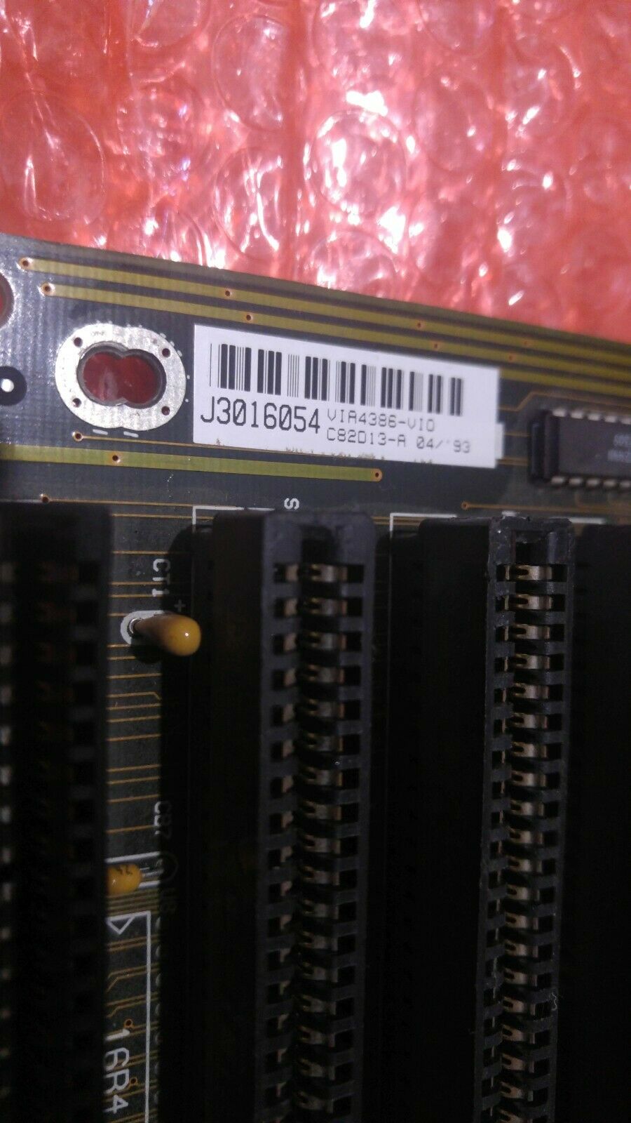
VIA4386-VIO
|
||||||
4386VC-HD
|
||||||
486-GAC-V
|
||||||
486-GIO-VP
|
||||||
486-GIO-VT
|
||||||
486-GIO-VT2
|
||||||
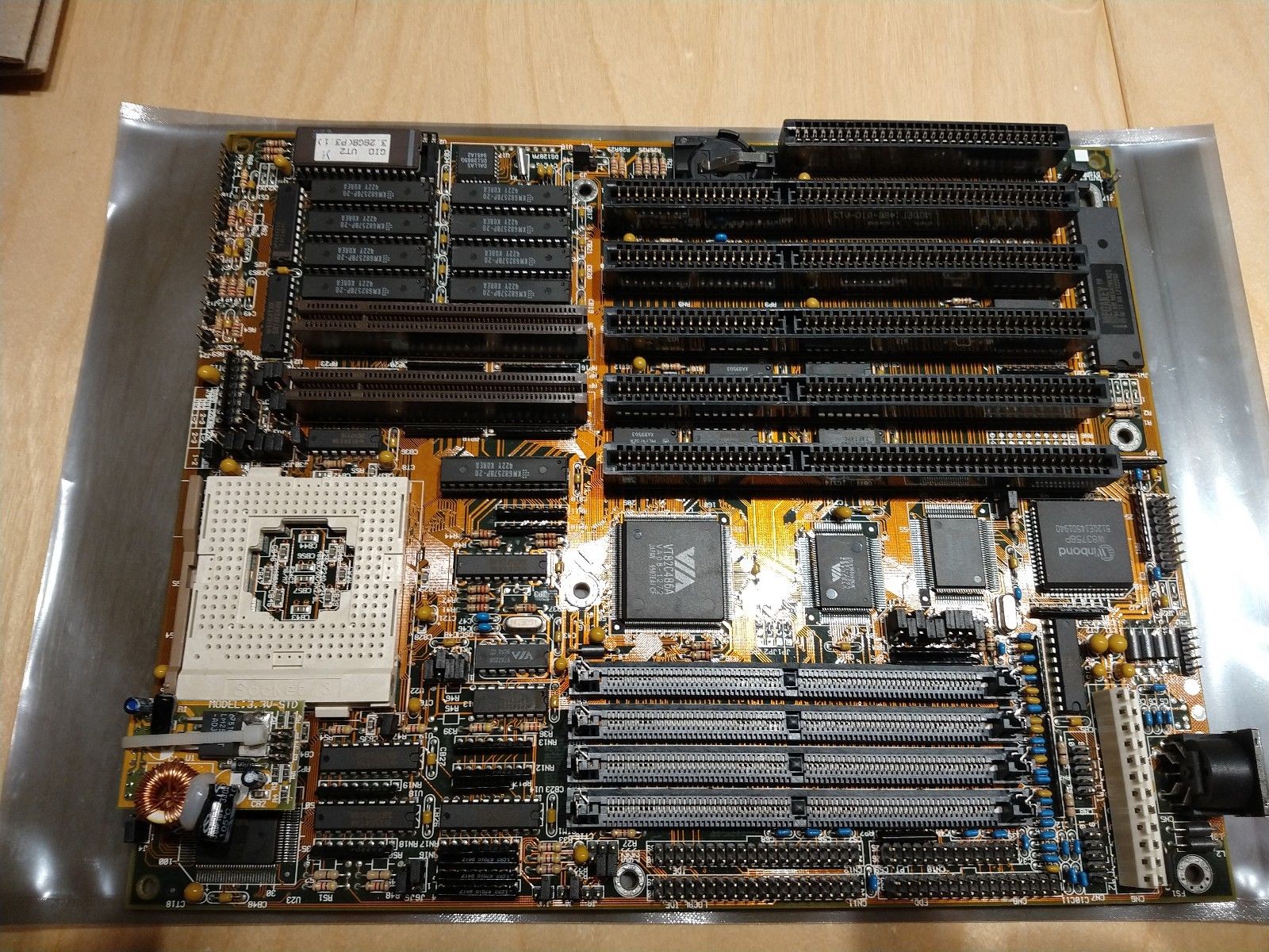
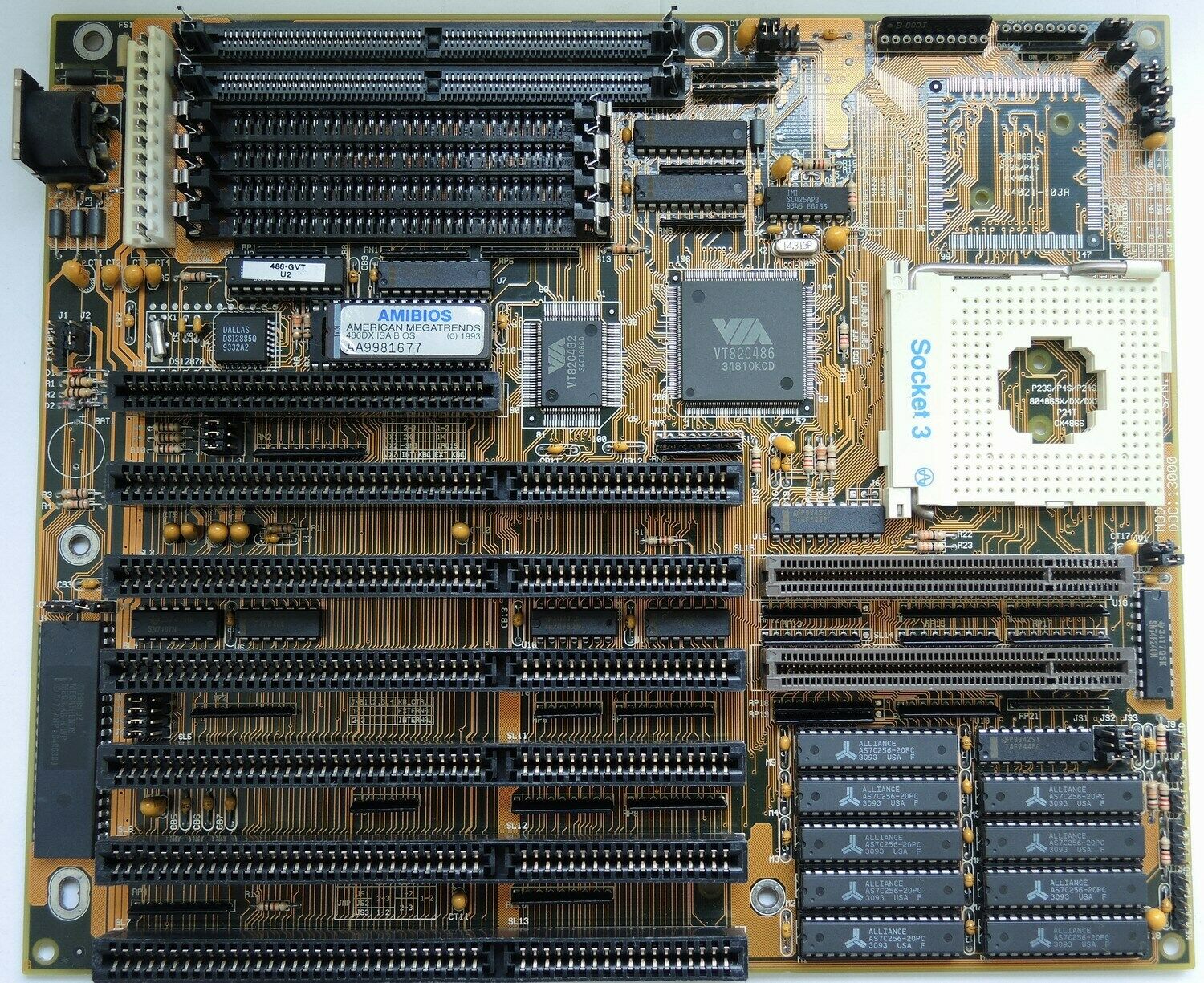
486-GVTYear: ? User Manual
|
||||||
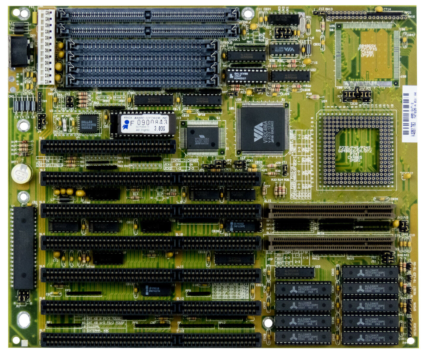
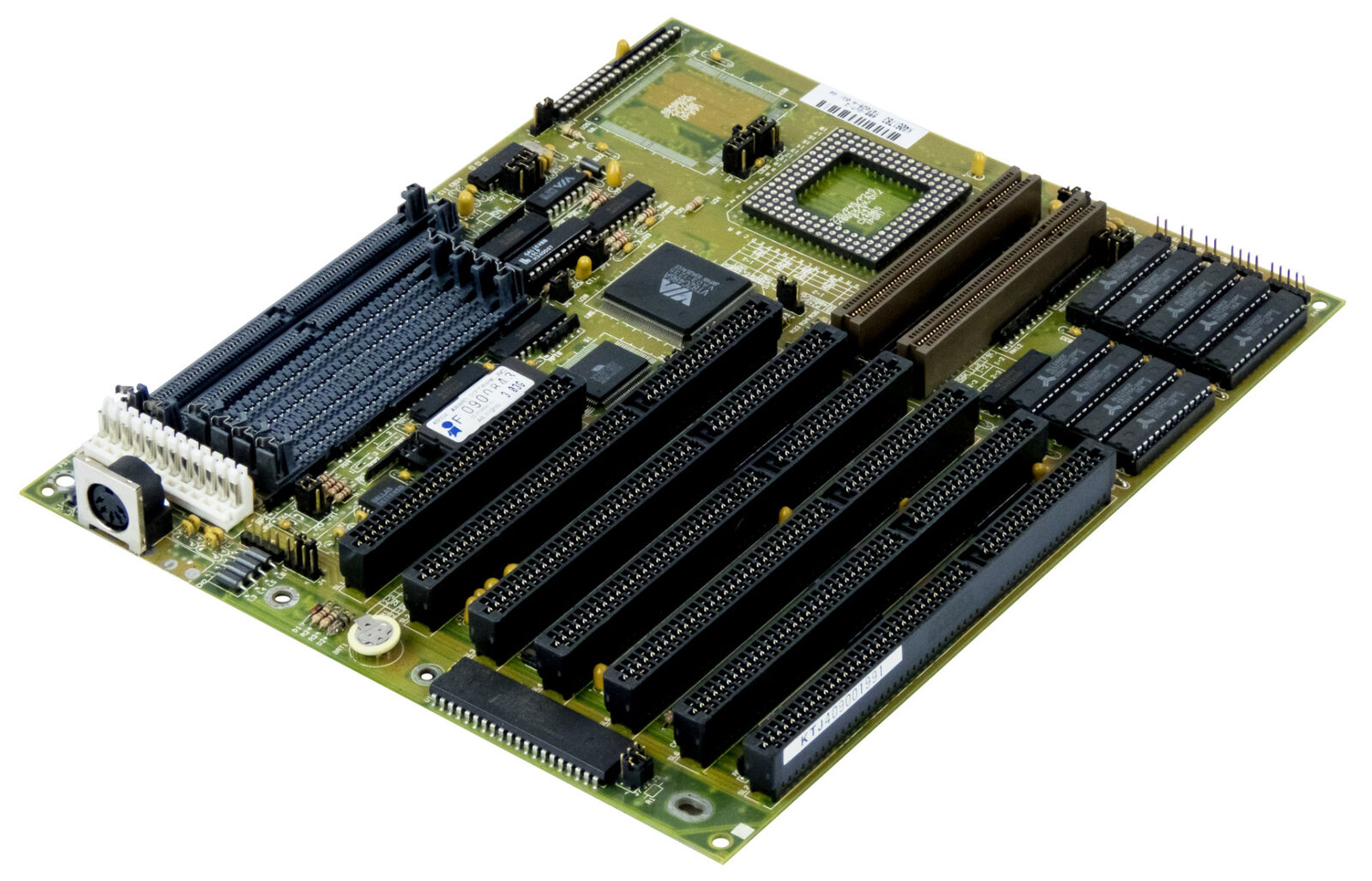
486-GVT-2
|
||||||
486-PAK-2Year: ? User Manual |
||||||
486-PIO-2Year: ? User Manual |
||||||
486-PIO-3
|

| Hercules Dynamite 128 | 44 MB/sec |
| Matrox Millennium (MGA2064) | 43 MB/sec |
| Elsa Winner 1000 (S3 Trio64V+) | 44 MB/sec |
486-POS
Year: ?
Type:
Form Factor:
Chipset:
Slots:
Memory:
User Manual
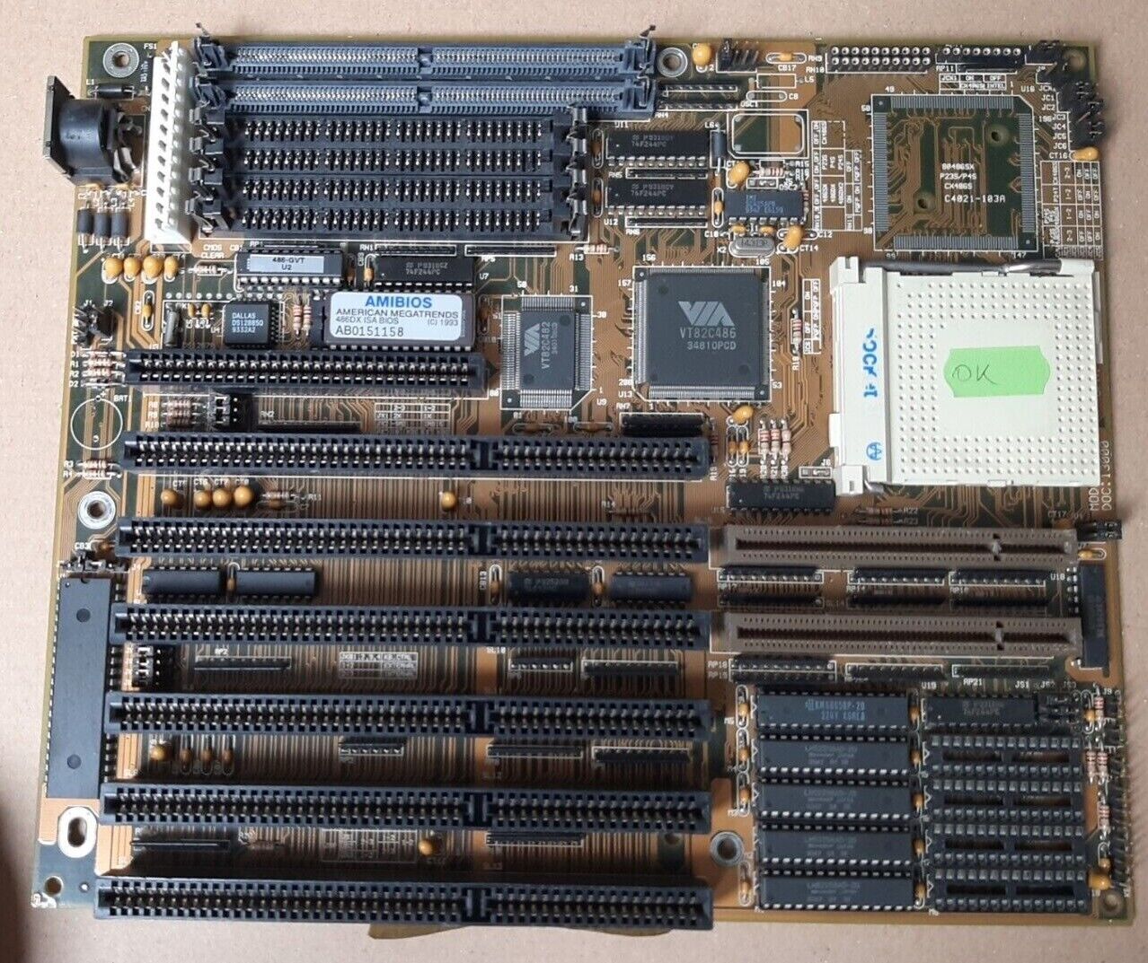
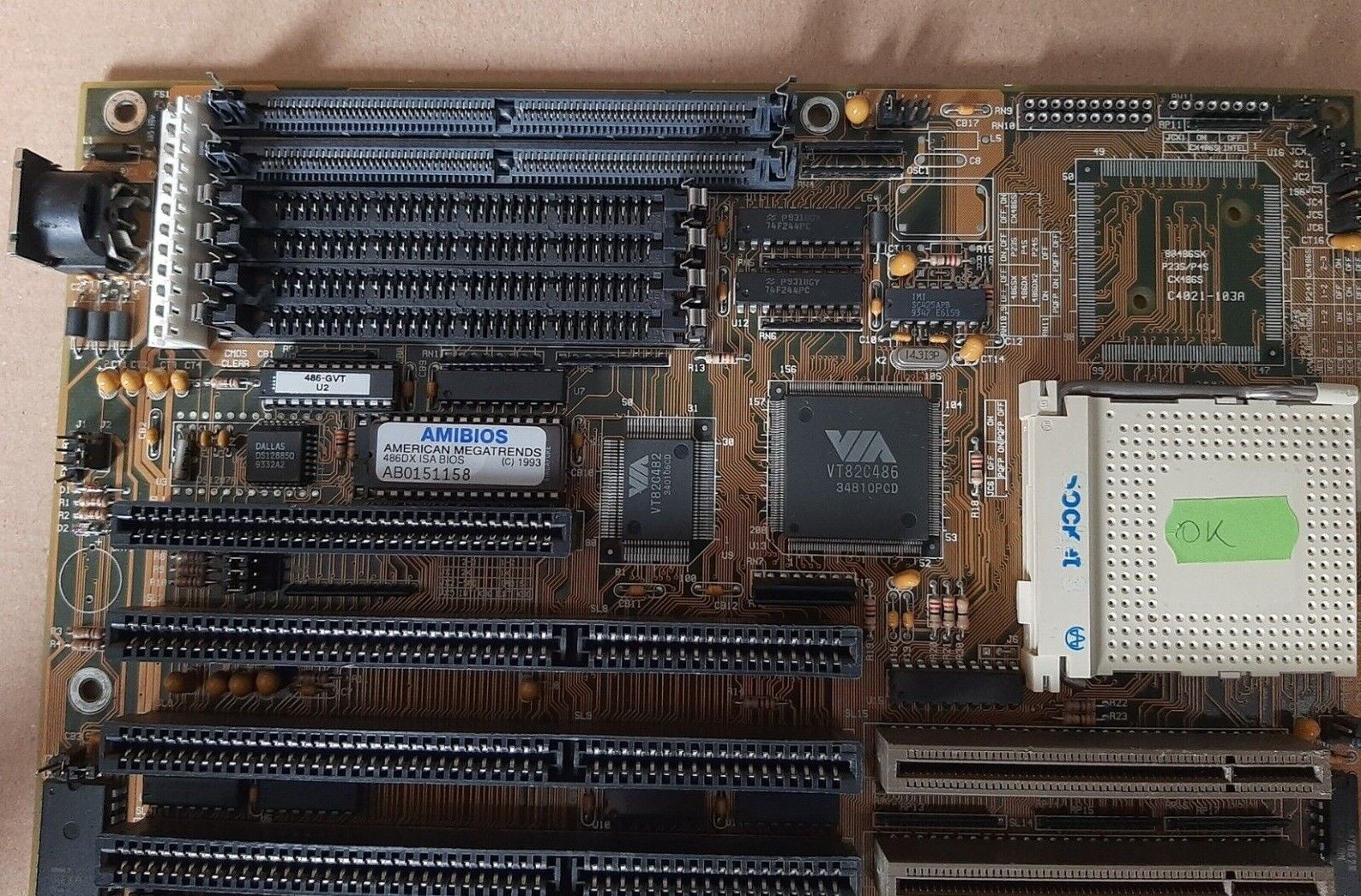
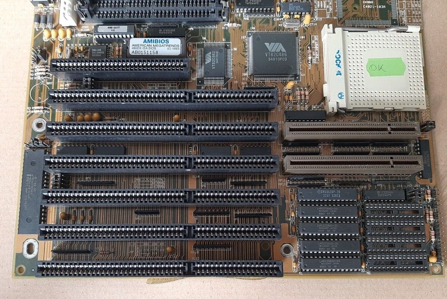
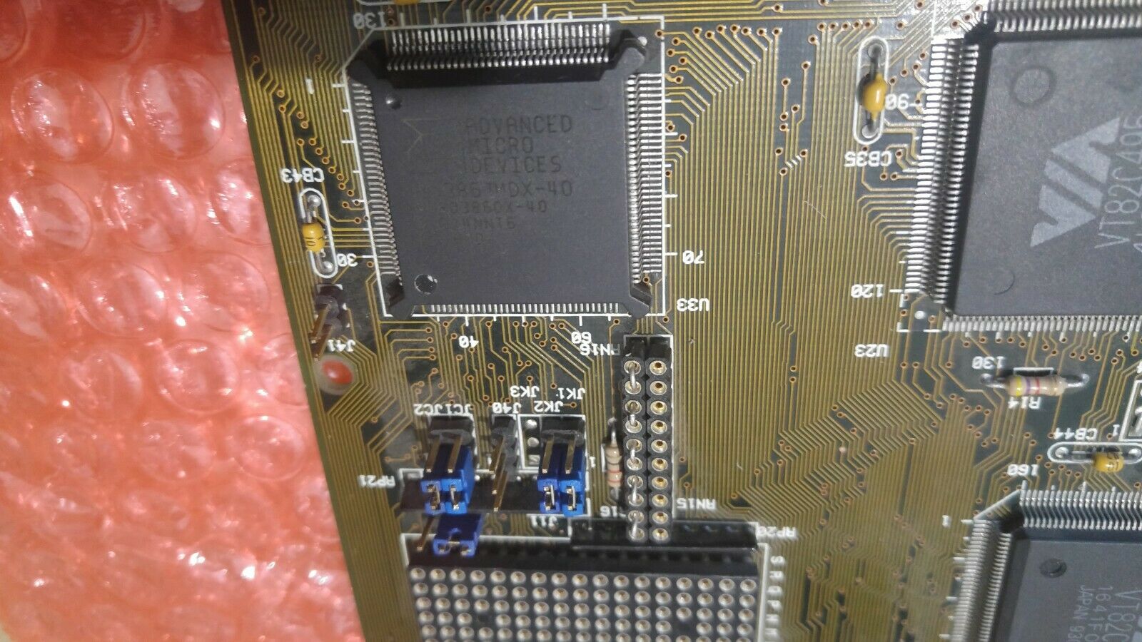
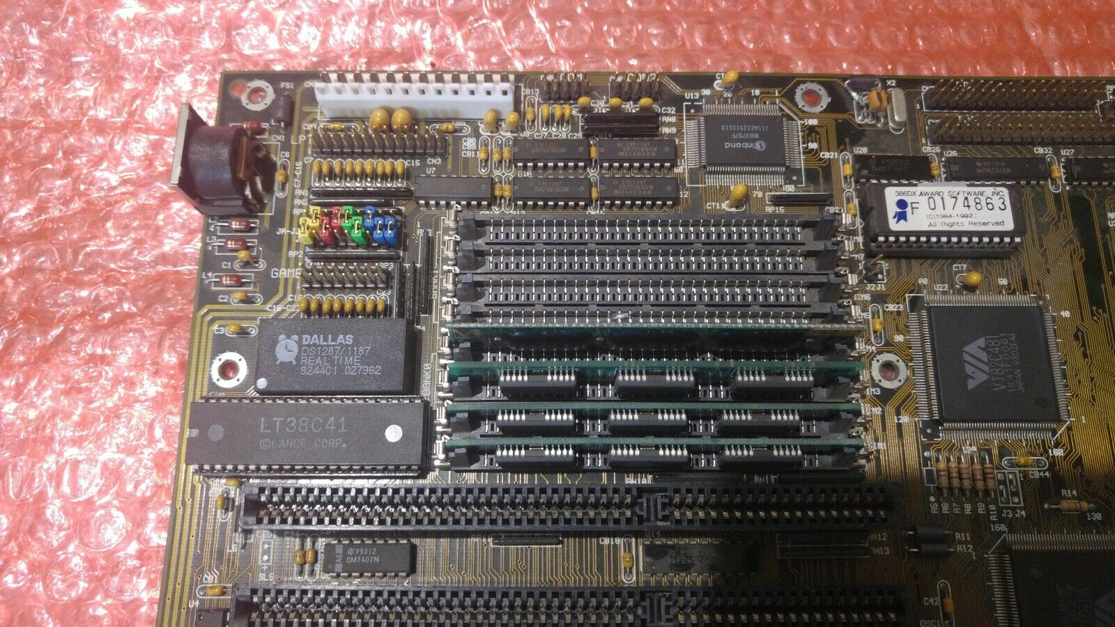
486-PVT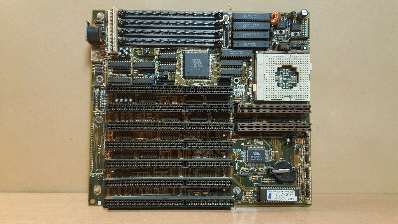
Year: ?
Type: Socket 3
Form Factor: AT
Power Connector: AT
Chipset: VIA 82C496G/82C406
Slots: 7 x 16-bit ISA, 2 x VLB
Memory: 4 x 72-pin SIMM
BIOS: Award
User Manual
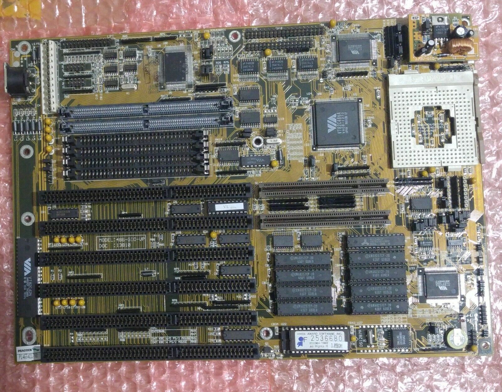
486-PVT-IO
Year: ?
Type:
Form Factor:
Chipset:
Slots:
Memory:
BIOS: Award v4.50G
User Manual
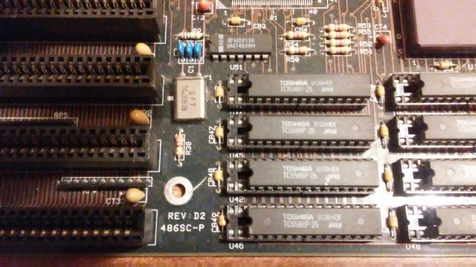
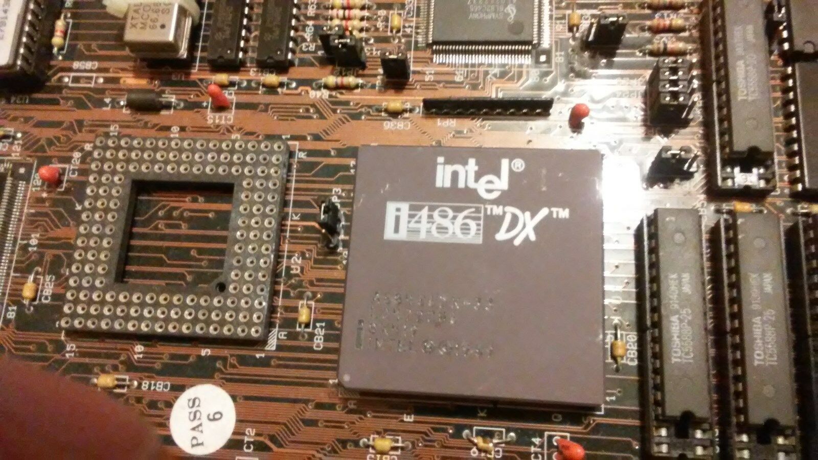
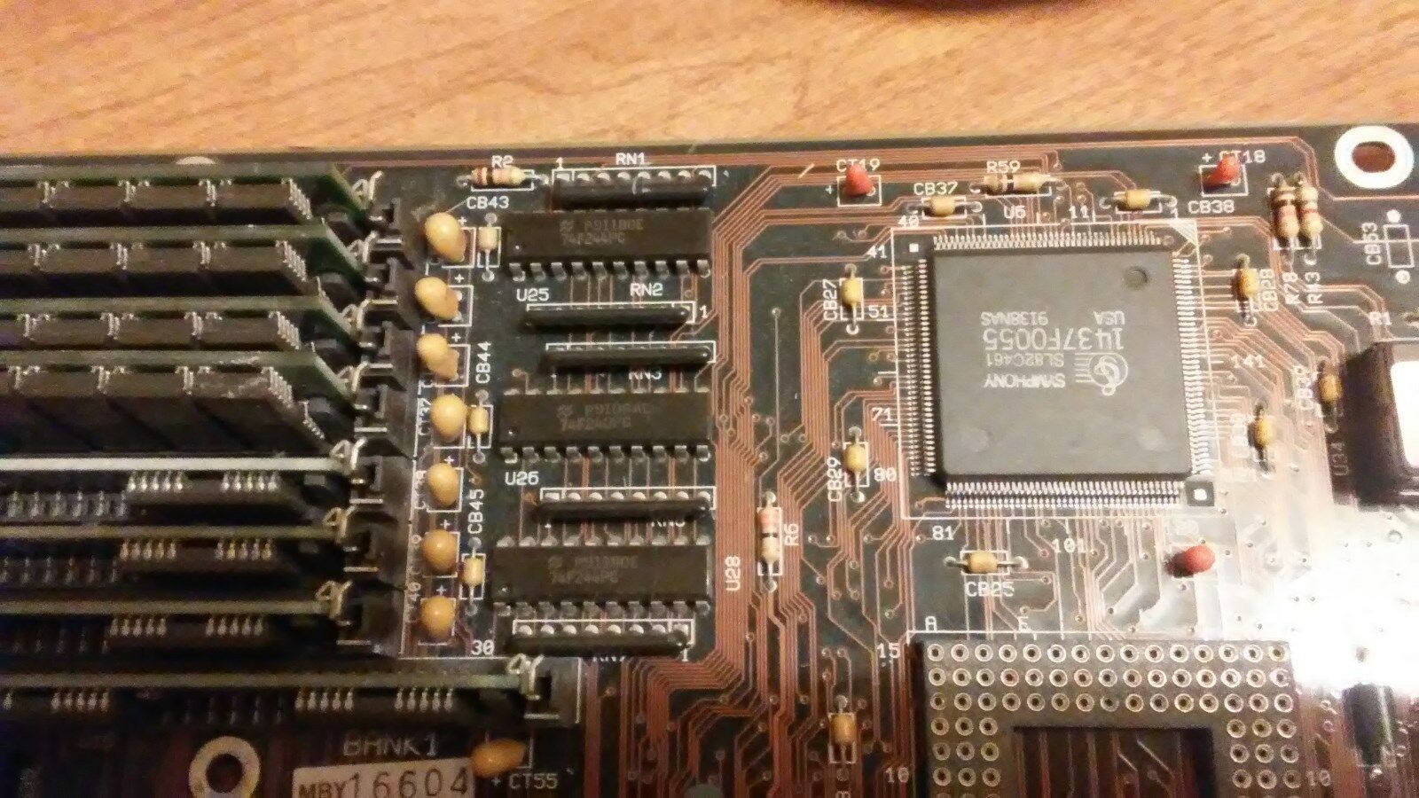
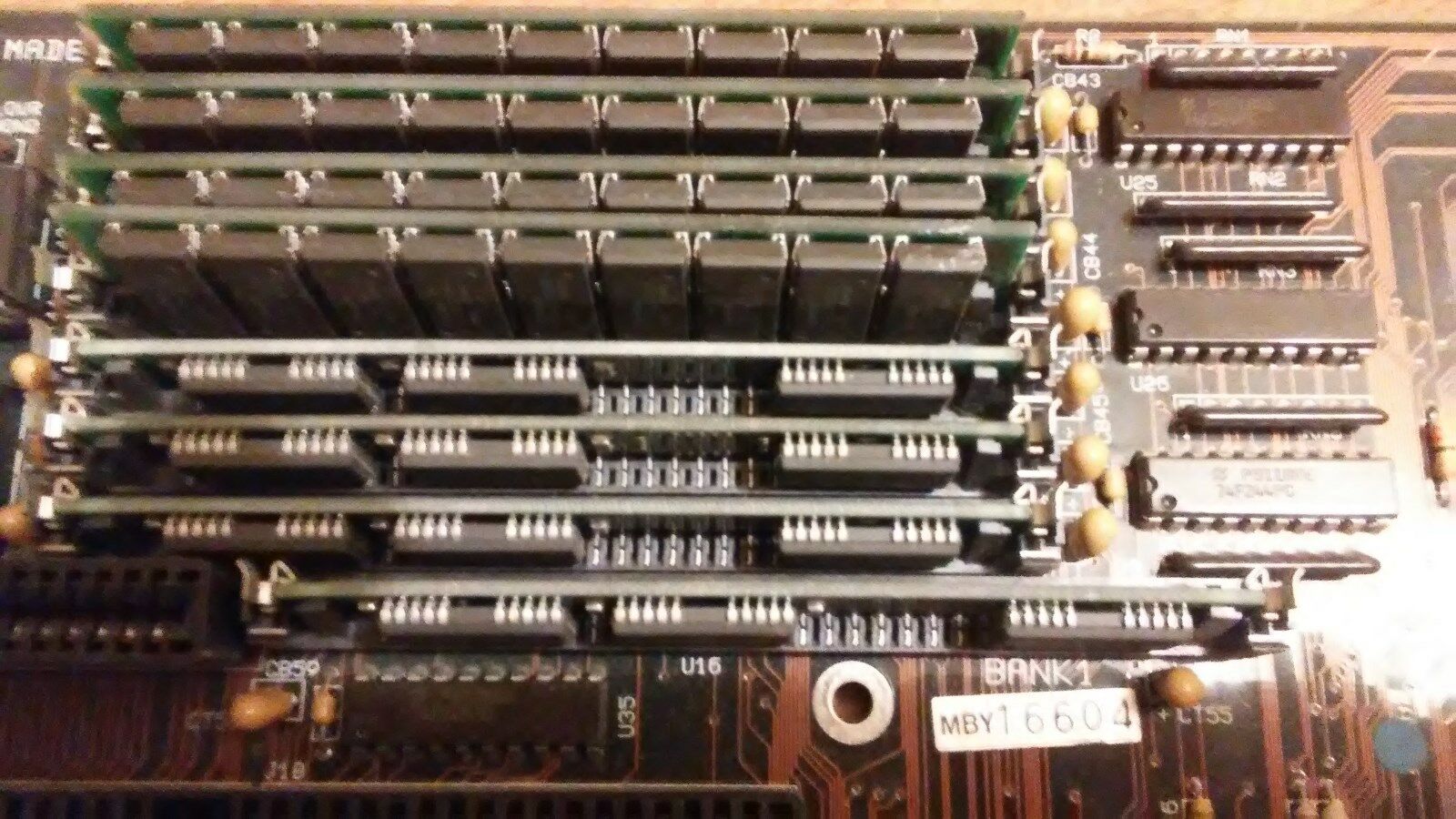
486SC-P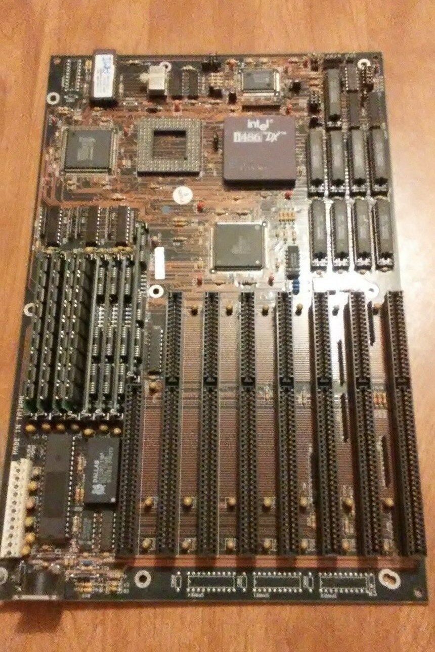
Year: 1991
Type: Socket 3
Form Factor: Baby AT
Chipset: Symphony SL82C461
BIOS: AMI
Slots: 7 x 16-bit ISA, 1 x 8-bit ISA
Memory: 8 x 30-pin SIMM (2 banks)
Known Board Revisions: D2
More Images
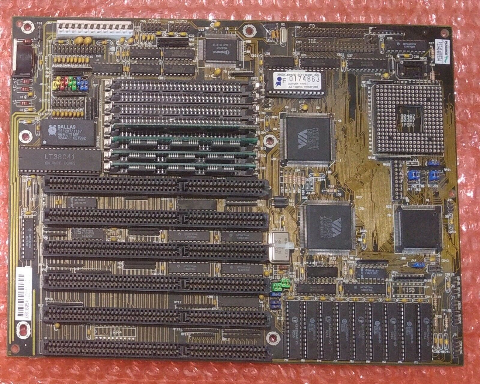
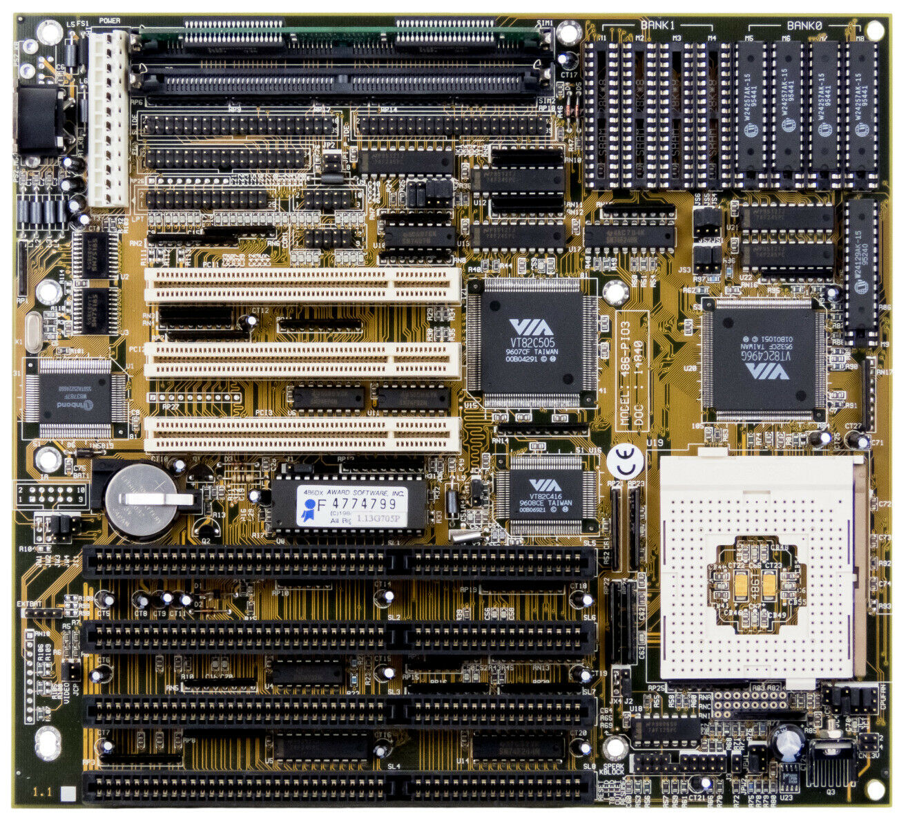
486-VIP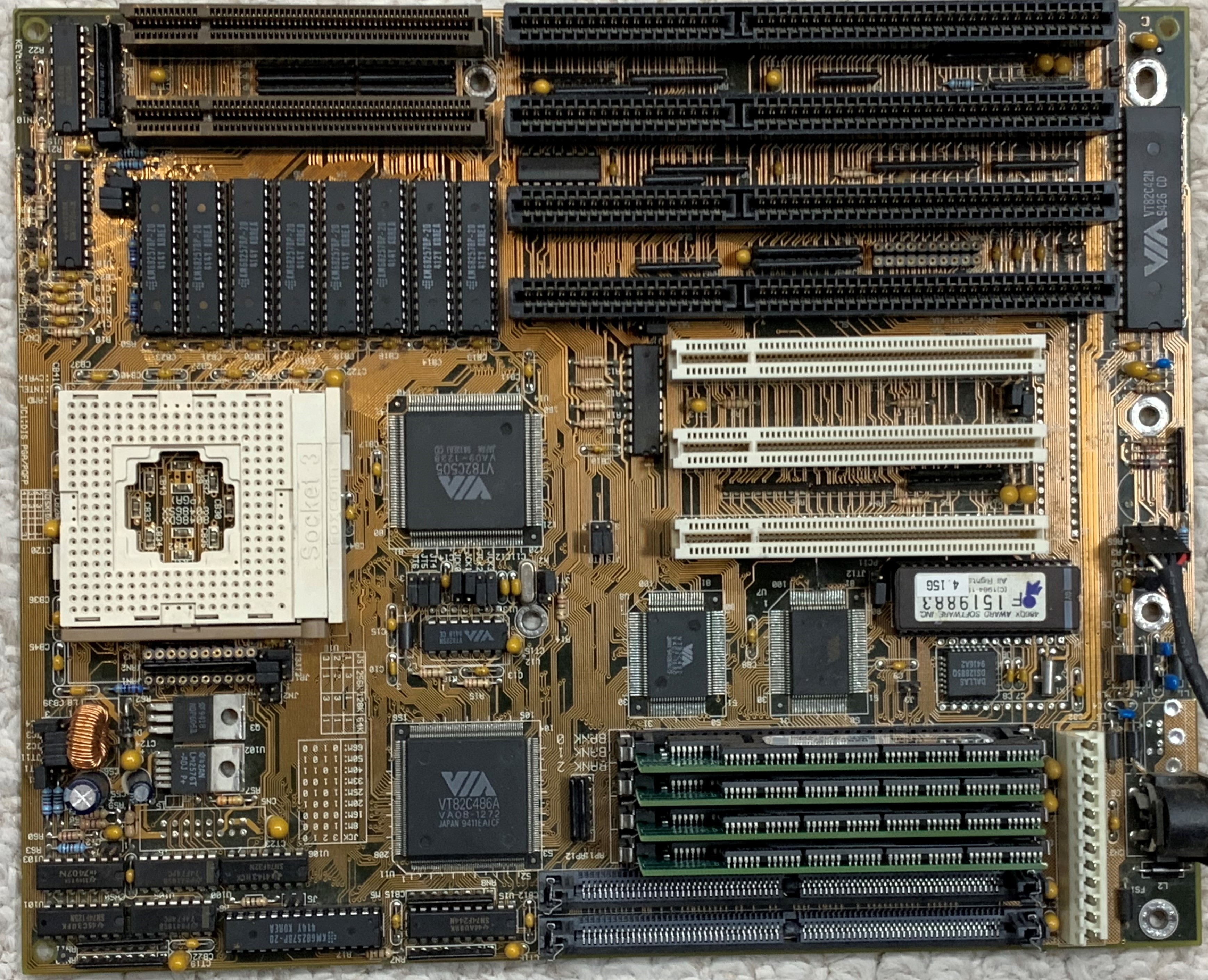
Year: 1994
Type: Socket 3
Form Factor: Baby AT
Chipset: VIA 82C486
BIOS: Award v4.50G
Slots: 4 x 16-bit ISA, 2 x VESA Local bus, 3 x PCI
Memory: 4 x 30-pin SIMM, 2 x 72-pin SIMM
Known Board Revisions:
BIOS Strings:
05/19/94-VT82C505-2A4L4000-00
User Manual
Board picture courtesy of Doug Bell
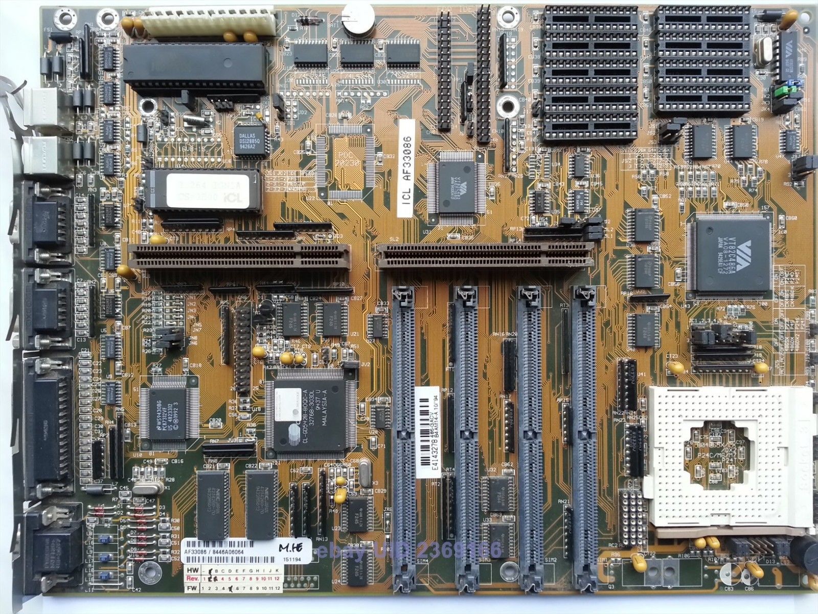
486-VIP-IO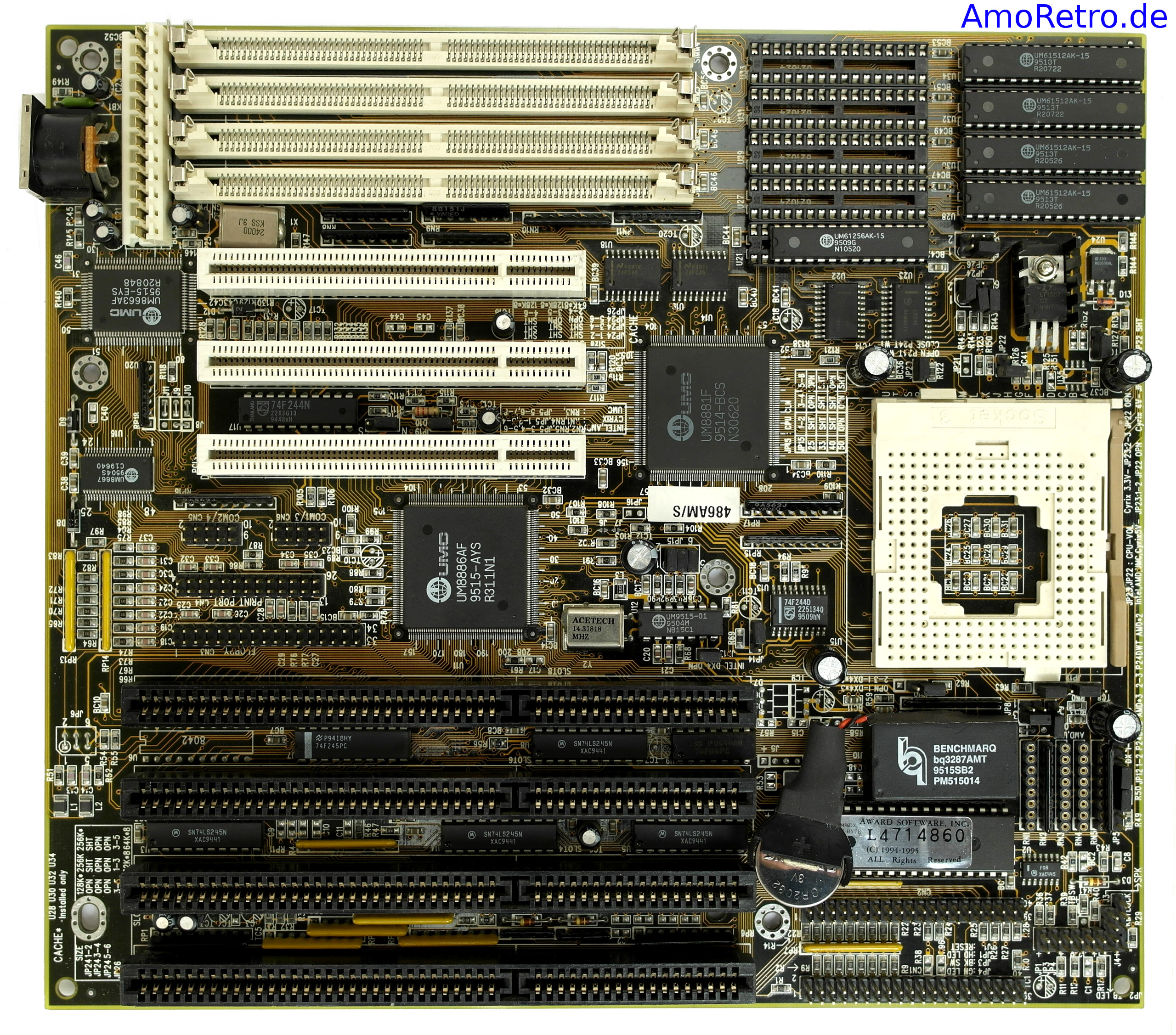
Year: 1994
Type: Socket 3
Form Factor: Baby AT
Chipset: VIA VT82C486A / VT82C505
Slots: ISA (3 x 16-bit), VLB (2), PCI (4)
Memory: 72-pin SIMM
BIOS: Award v4.50G
Tested maximum bus transfer rates with this board:
| Hercules Dynamite 128 | 17 MB/sec |
| Matrox Millennium (MGA2064) | 15 MB/sec |
| Elsa Winner 1000 (S3 Trio64V+) | 15 MB/sec |
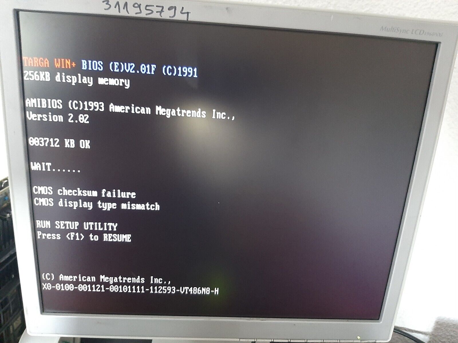
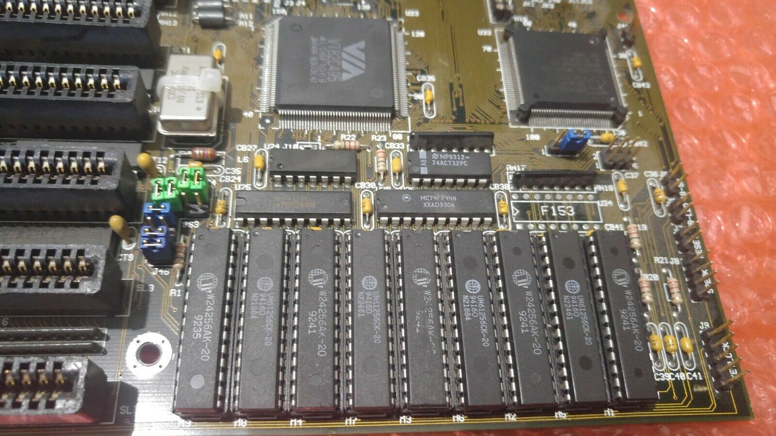
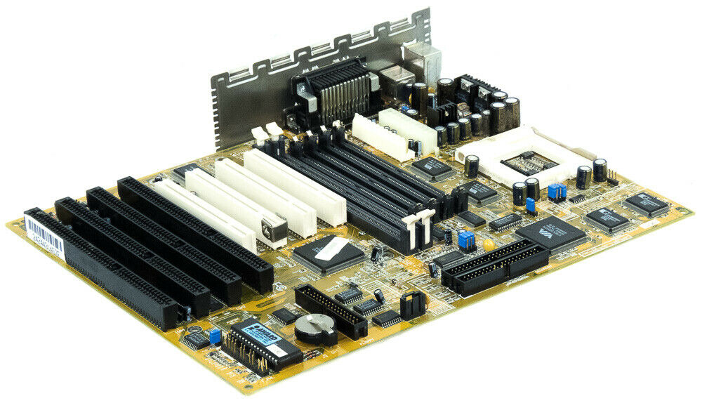
486-VIP-IO2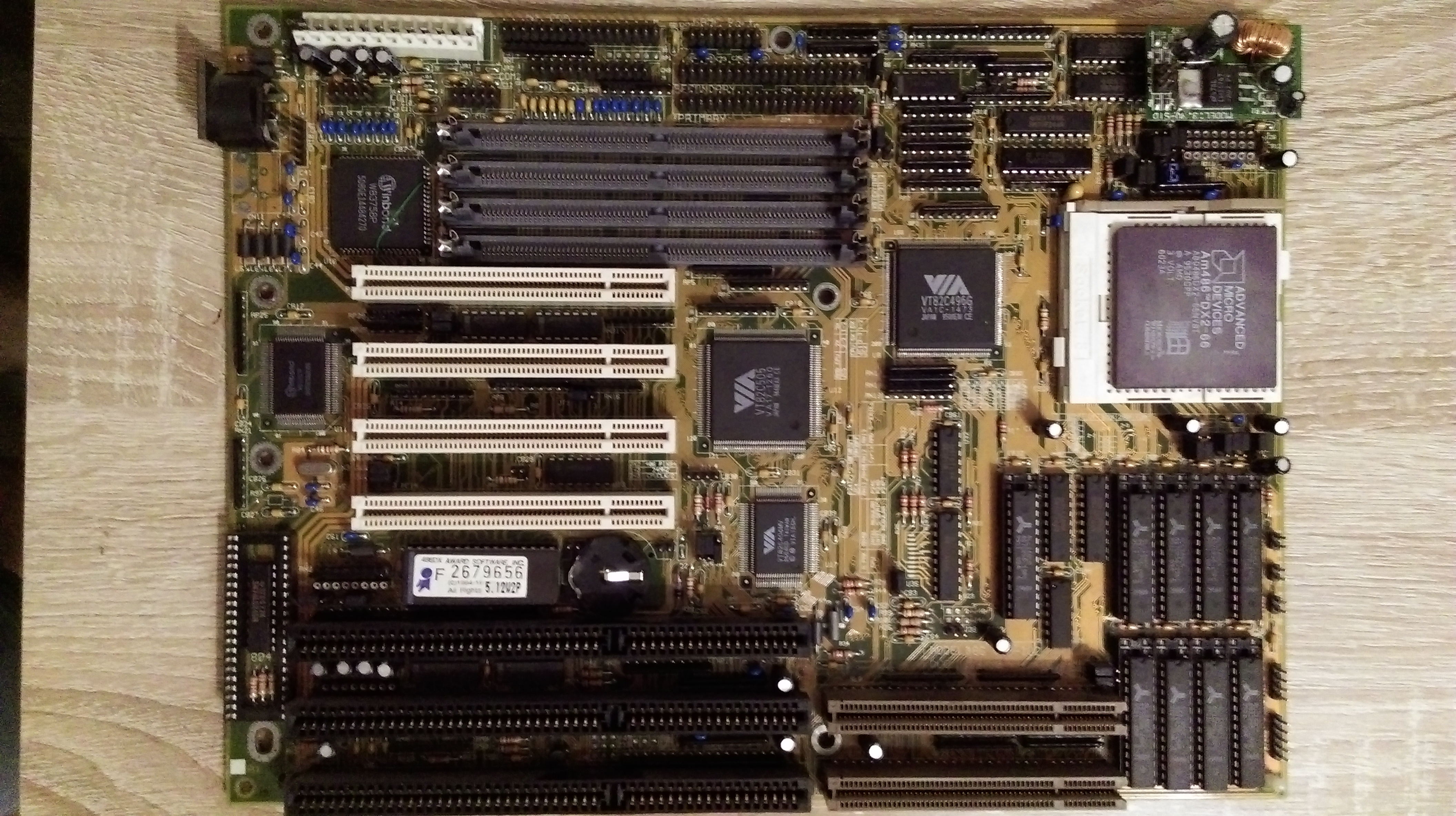
Year: 1995
Type: Socket 3
Form Factor: AT
Chipset: VIA VT82C496G / VT82C505
Slots: 3 x ISA (16-bit), 4 x PCI, 2 x VLB
Memory: 4 x 72-pin SIMM
This board is feature-rich, but the BIOS is ancient and is not flashable. I have three of these motherboards, and did a full review in April 2021.![]()
Tested maximum bus transfer rates with this board:
| Hercules Dynamite 128 | 44 MB/sec |
| Matrox Millennium (MGA2064) | 43 MB/sec |
| Elsa Winner 1000 (S3 Trio64V+) | 44 MB/sec |
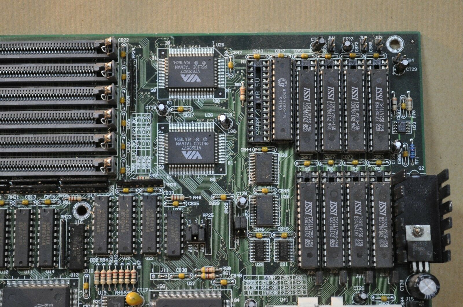
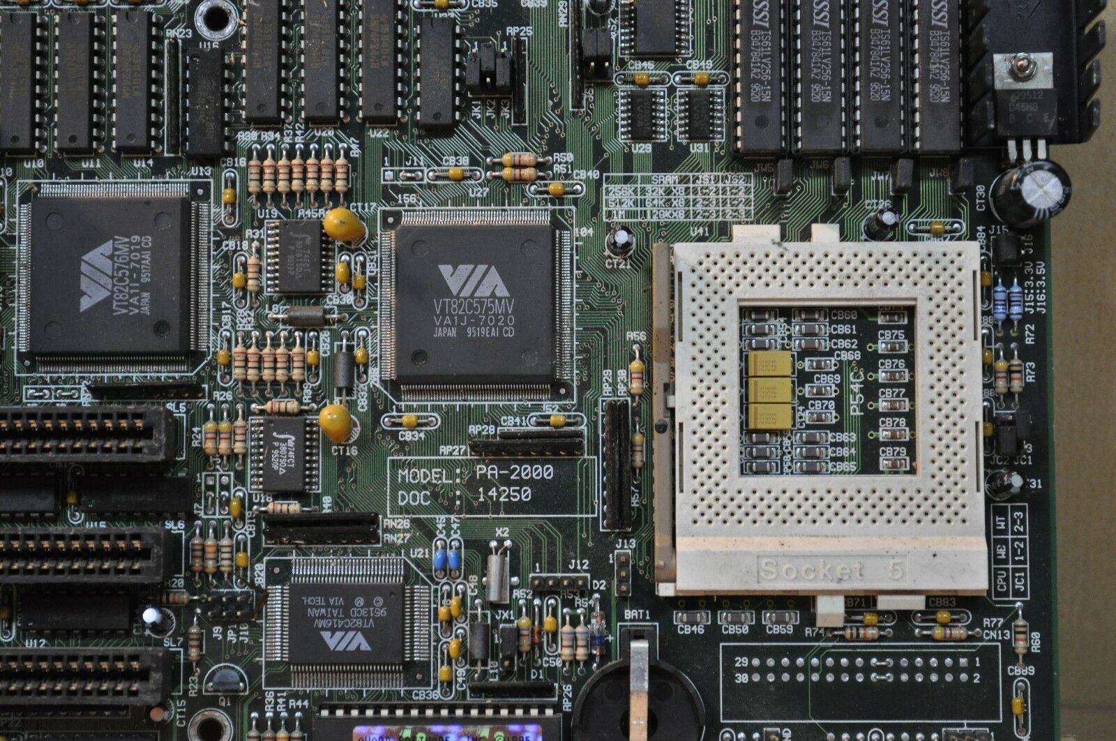
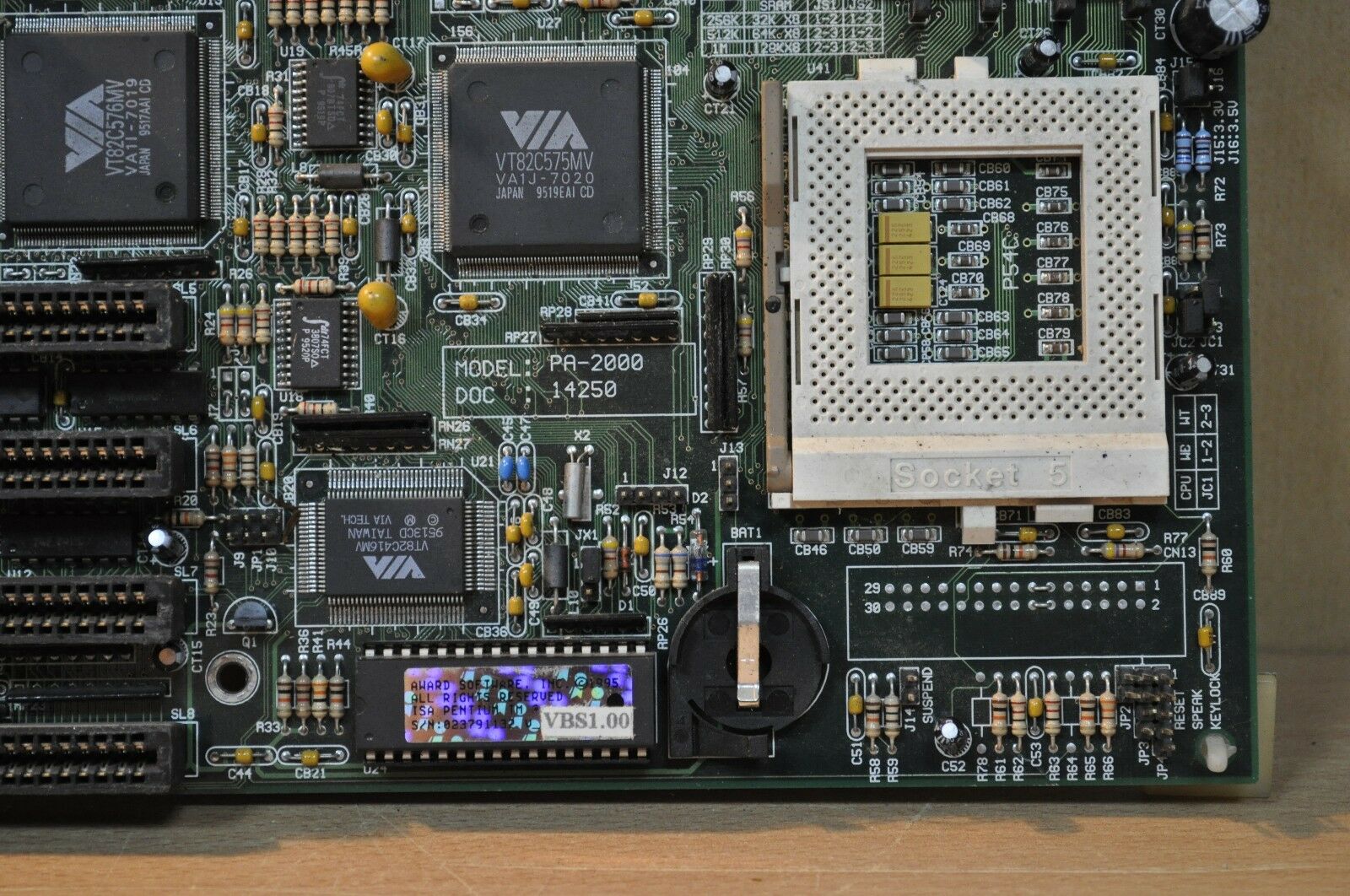
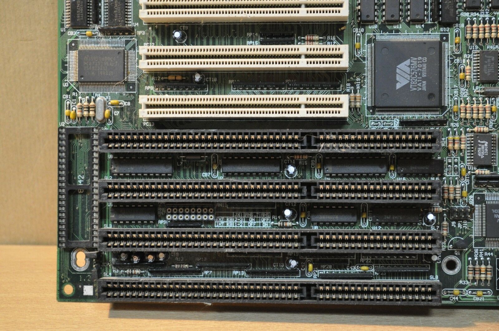
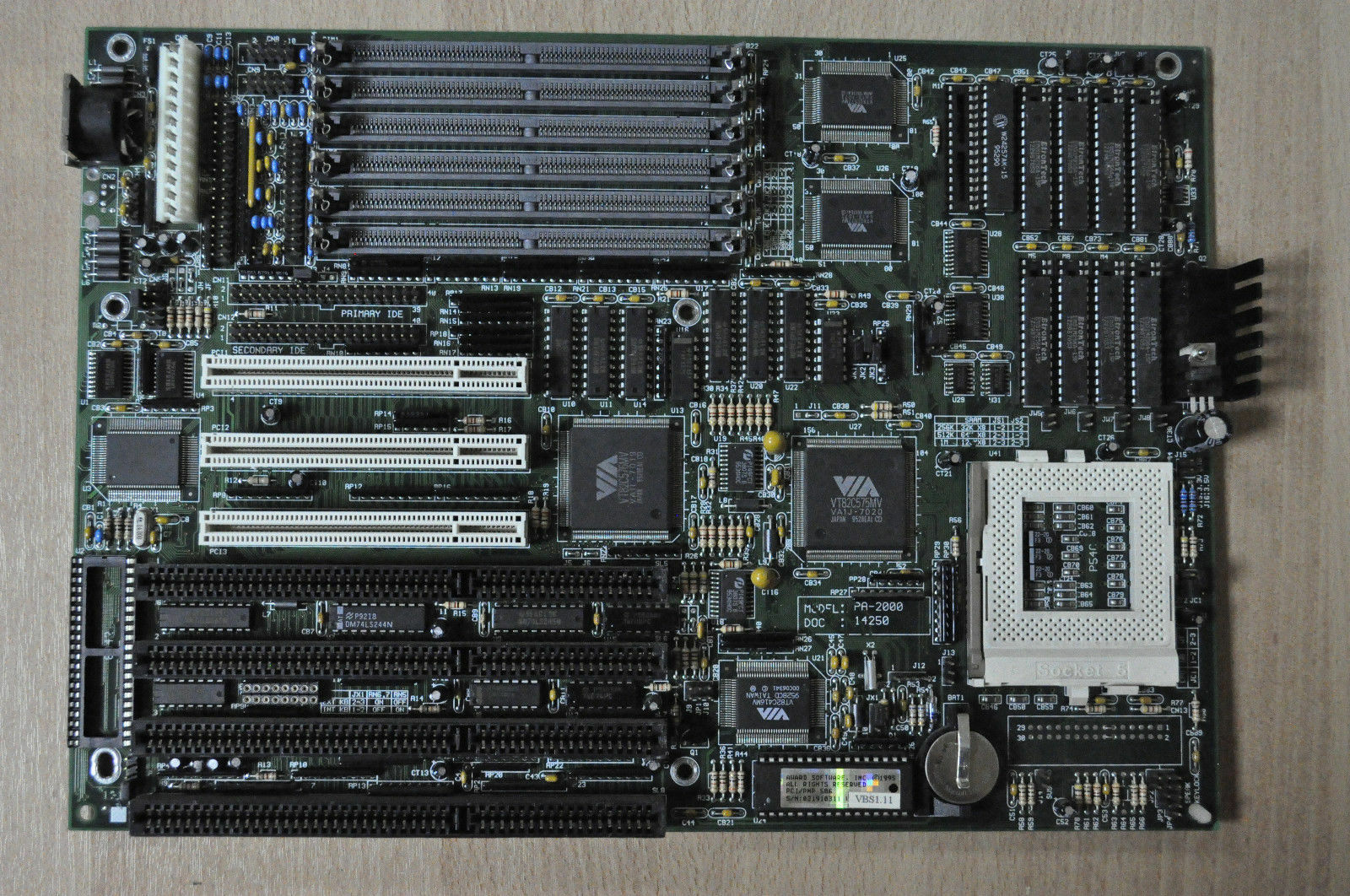
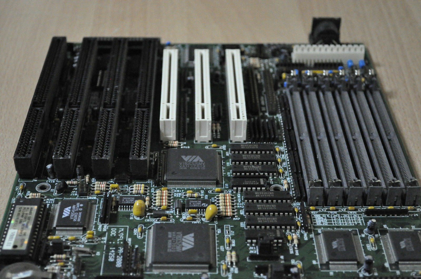
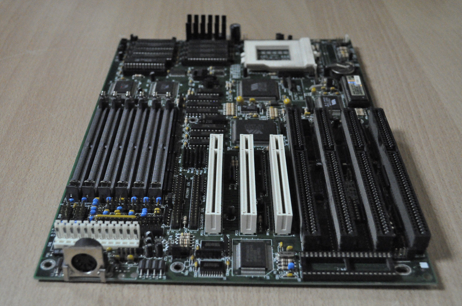
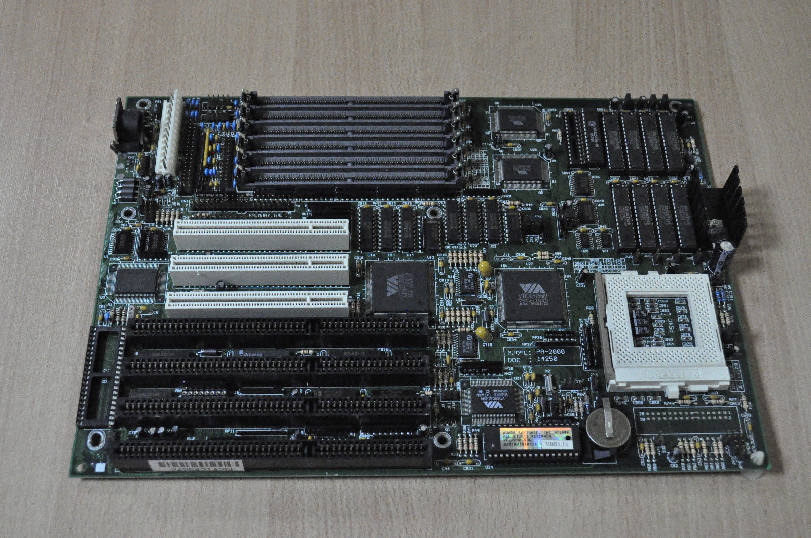
PA-2000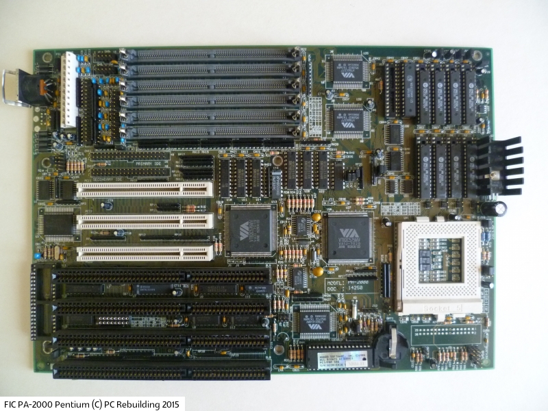
Year: 1995
Type: Socket 5
Form Factor: ATX
Chipset: VIA Apollo Master
Slots: 4 x ISA (16-bit), 3 x PCI
Memory: 6 x 72-pin DRAM SIMM, 192 MB max.
BIOS: Award 4.50G
Supports bus speeds of 50 or 66 MHz.
CPU clock speeds supported are 75-133 MHz (non-MMX).
User Manual
User Manual Update
Jumper Settings
More Images
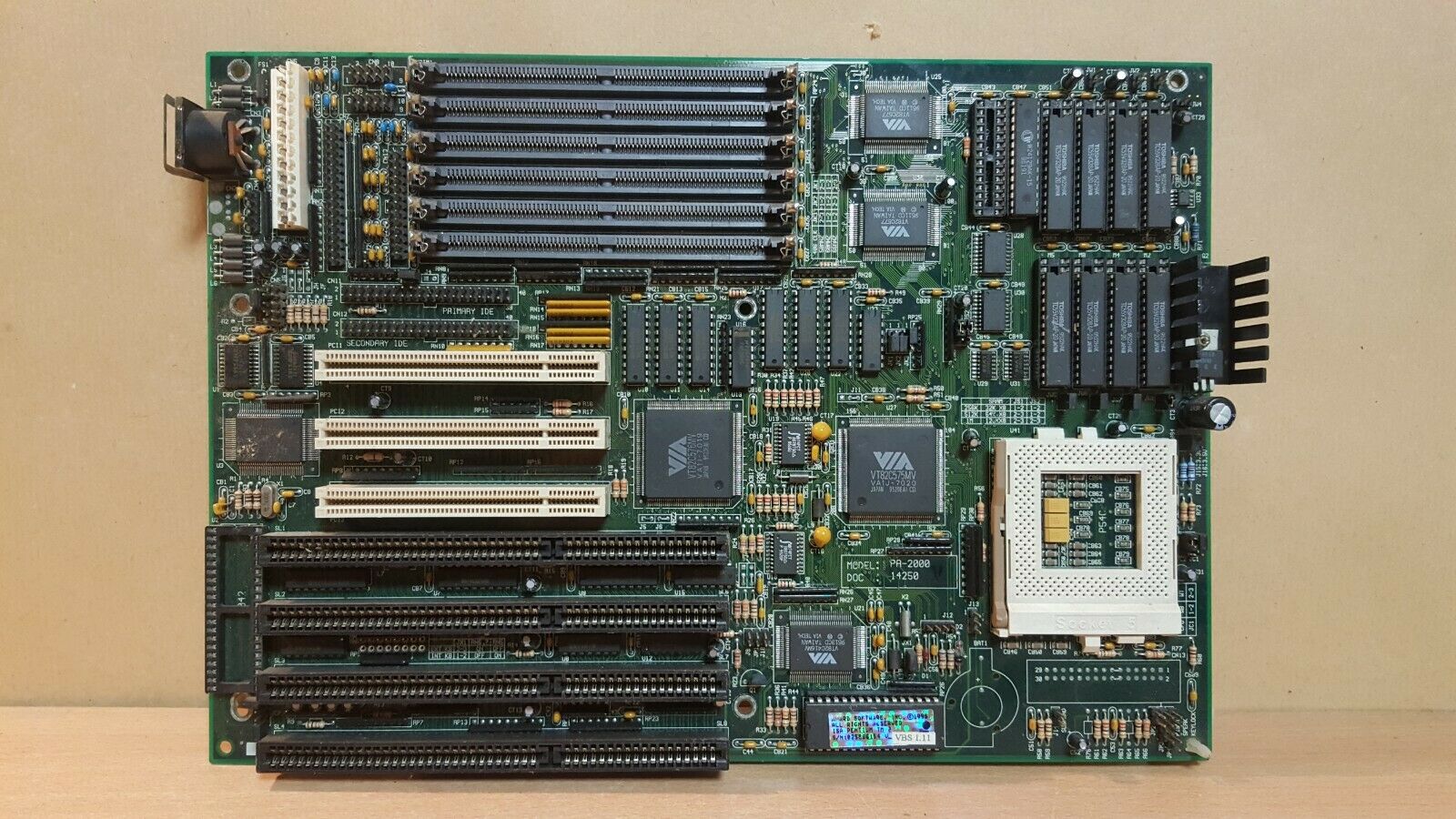
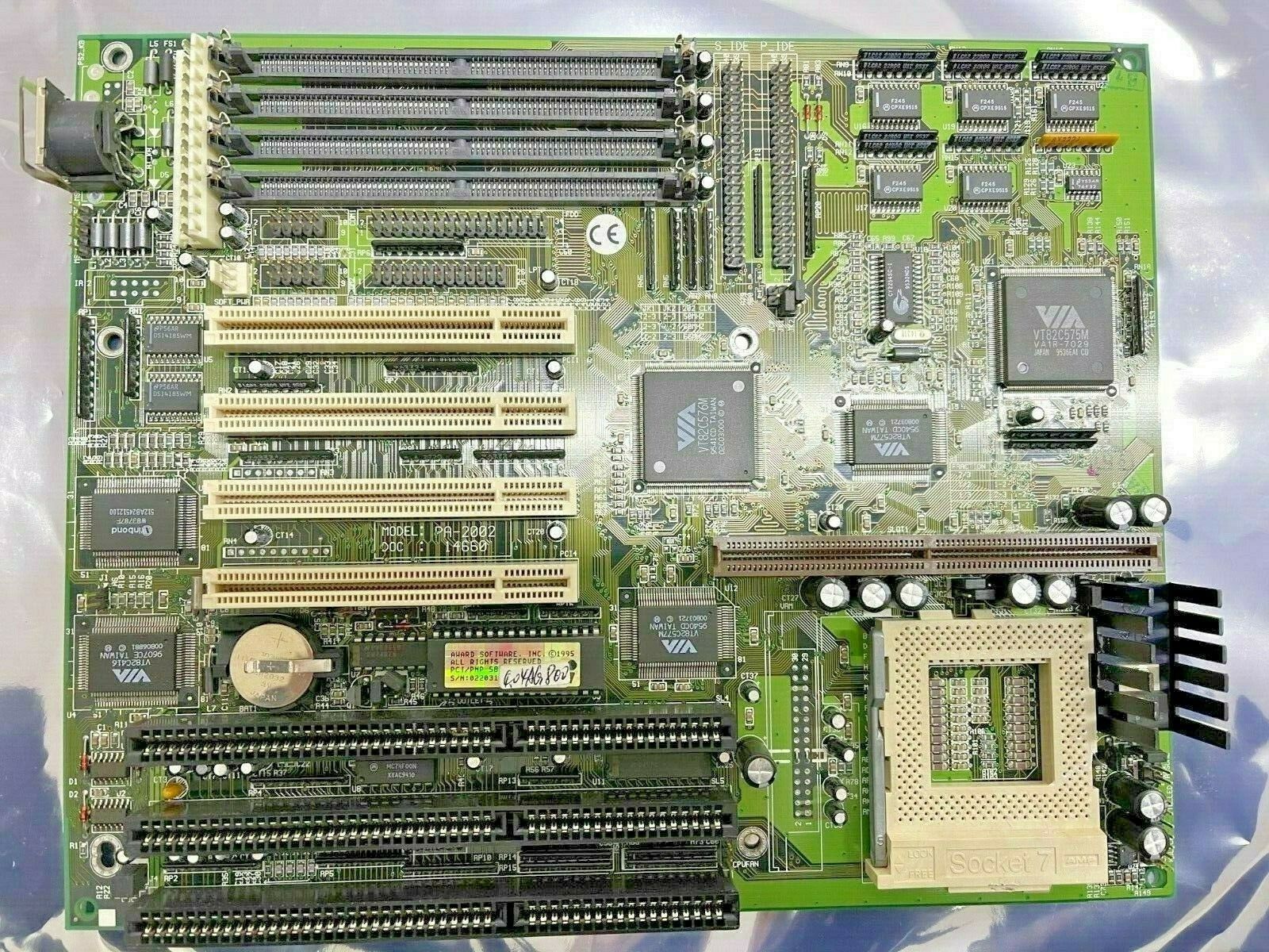
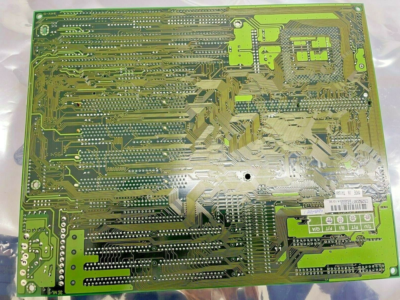
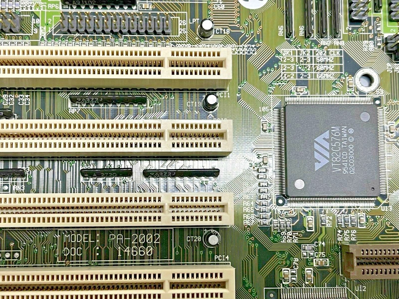
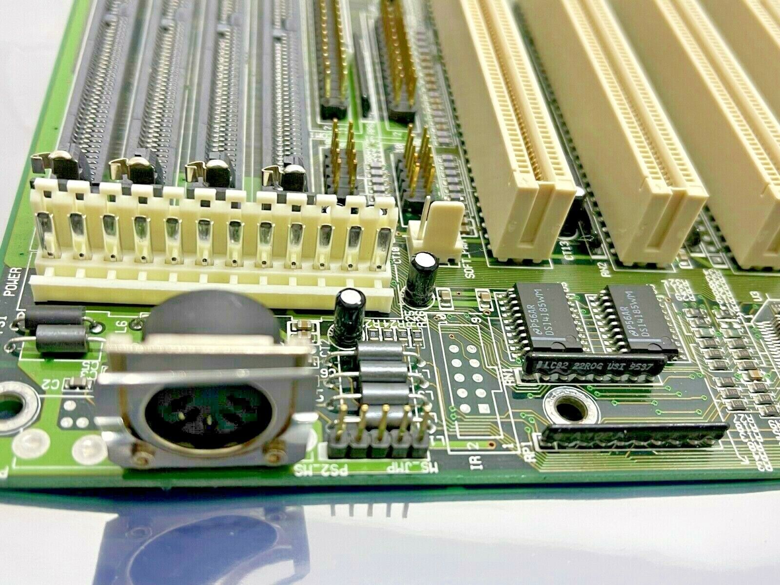
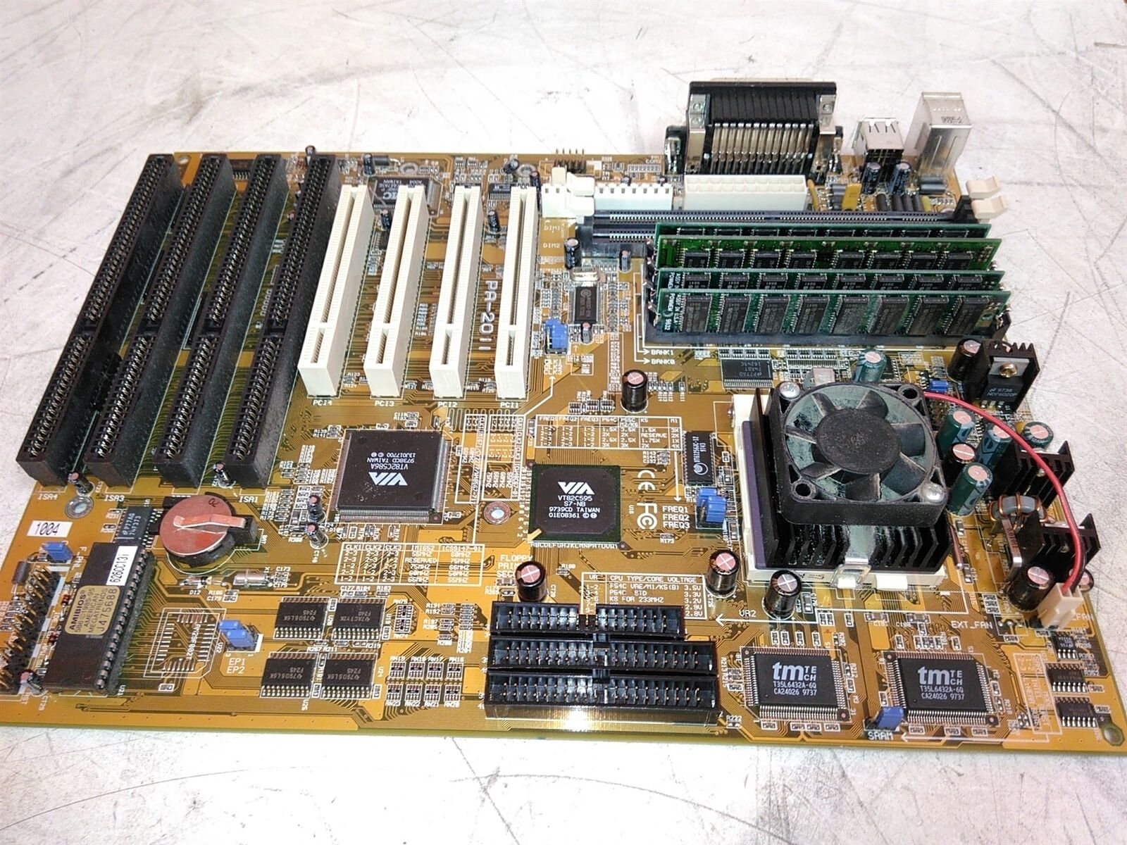
PA-2002
Year: 1996
Type: Socket 7
Form Factor: ATX
Power Connector: AT
Chipset: VIA Apollo Master
Slots: 3 x ISA (16-bit), 4 x PCI, 1 x COAST
Memory: 4 x 72-pin DRAM SIMM, 128 MB max.
BIOS: Award 4.51PG
Known Board Revisions: 1.21 (PA2002C)
Supports bus speeds of 50 or 66 MHz.
CPU clock speeds supported are 75 - 200 MHz.
This board also has the COAST (Cache On A STick) module slot (160-pin). 256 KB L2 cache onboard.
Supports Pentium classic up to 200 MHz, IBM 6x86 up to P166, or AMD K5 up to PR166. Pentium MMX is only supported with the use of a voltage regulator.
Redhill said this about the PA-2002: "A popular board for a while, forerunner of the excellent PA-2005, and one of the first half-decent non-Intel chipset mainboards for Socket 7, but not a board to love by any means: these were tricky to set up right and fussy about RAM and CPU matching, although perfectly practical once you got the hang of them. The PA-2002 was at its best with a Pentium and could be problematic with Cyrix or AMD CPUs in those early days. We preferred the then-current Chaintech 5IEM or QDI Explorer II for the 6x86. One unexpected bonus of the Apollo chipset, almost unique amongst Socket 7 boards, is that the memory management unit could address a single 72-pin SIMM module if required. This imposed a slight performance penalty, so it was usual to fit RAM in pairs.".
The PA-2002C board supports the Cyrix 6x86 CPUs from P120+ to P150+.
User Manual
Jumper Settings
BIOS Update 205C800 dated 03/11/96
More pics: 1
More Images
PA-2003
Year: 1996
Type: Socket 7
Form Factor: ?
Chipset: ?
Slots:
Memory:
BIOS: Award
BIOS Dates: 02/28/96
Known Board Revisions: 1.3
The PA-2003 board supports the Cyrix 6x86 CPUs from P120+ to P166+.
PAC-2003
Year: 1996
Type: Socket 7
Form Factor: Custom
Chipset: VIA
Slots: 1 riser slot
Memory: 4 x 72-pin SIMM
BIOS: Award
BIOS Dates: -
Known Board Revisions: -
The PAC-2003 board was a proprietary board for an OEM. It uses a riser card for expansion slots.
It supports the Pentium MMX range
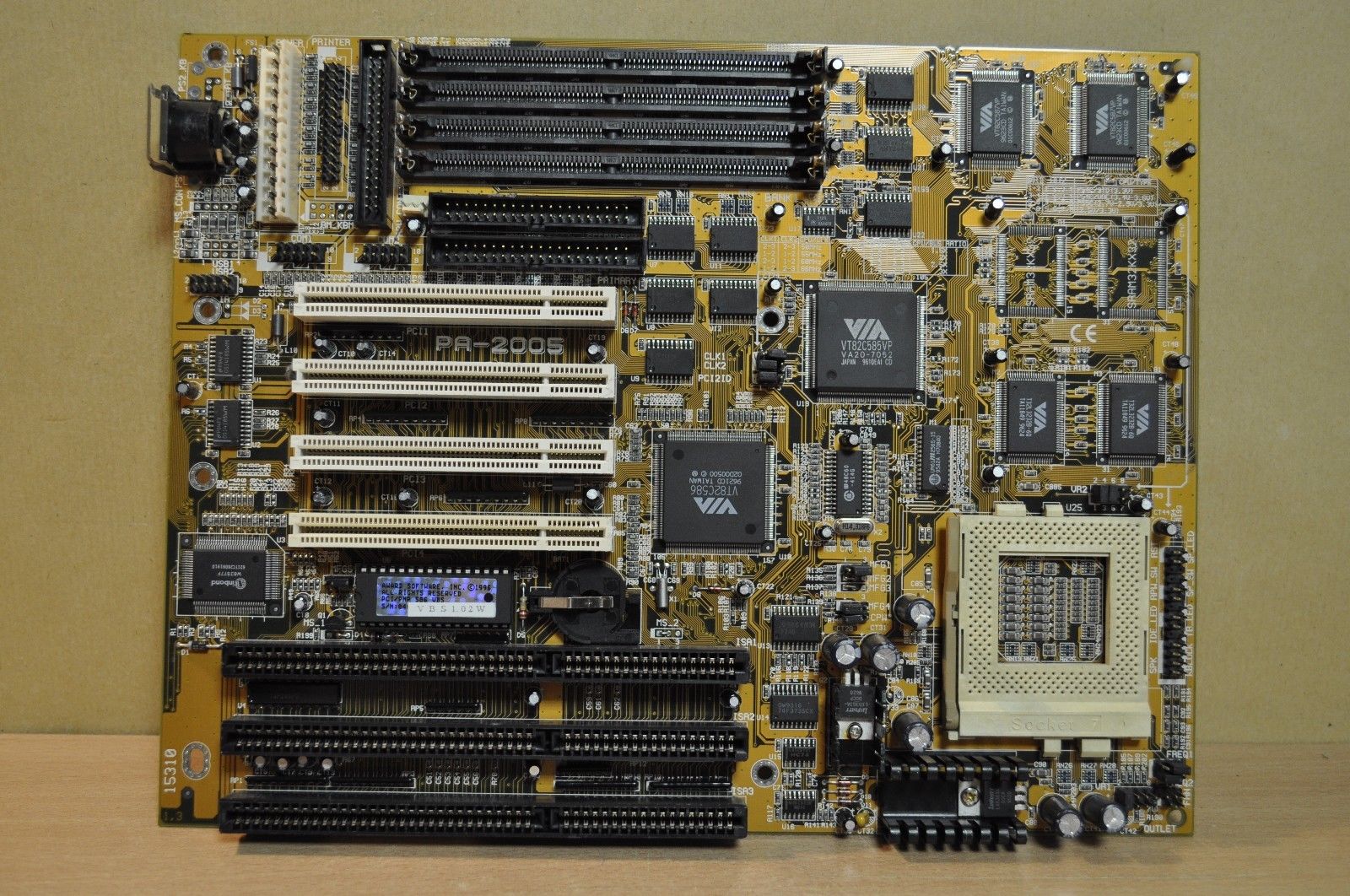
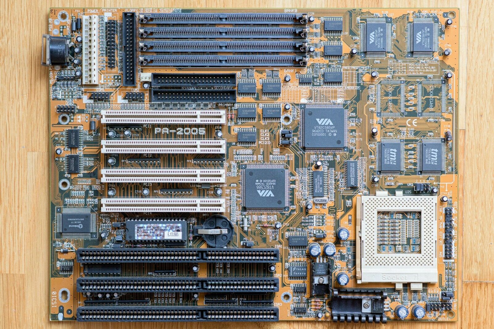
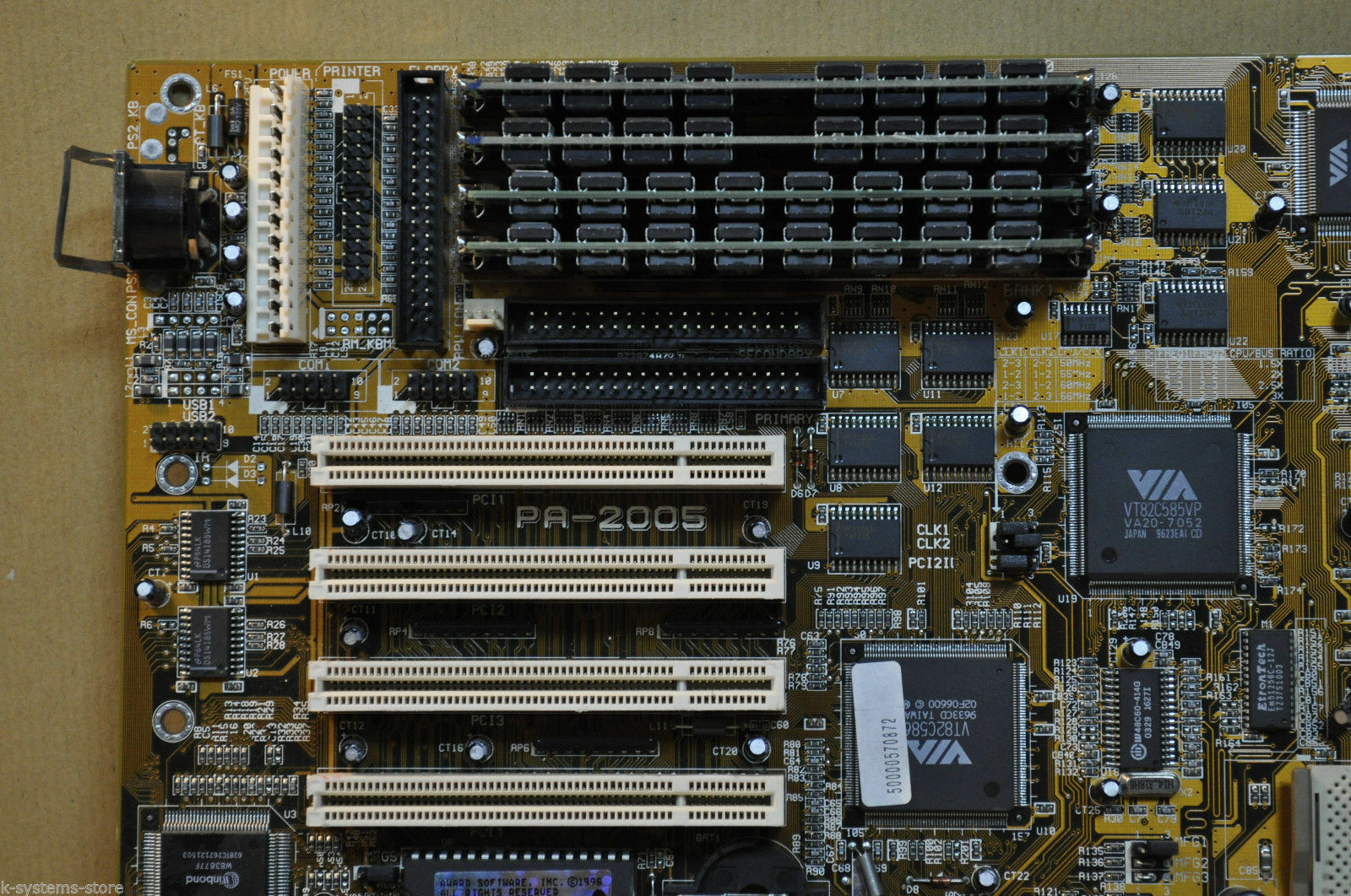
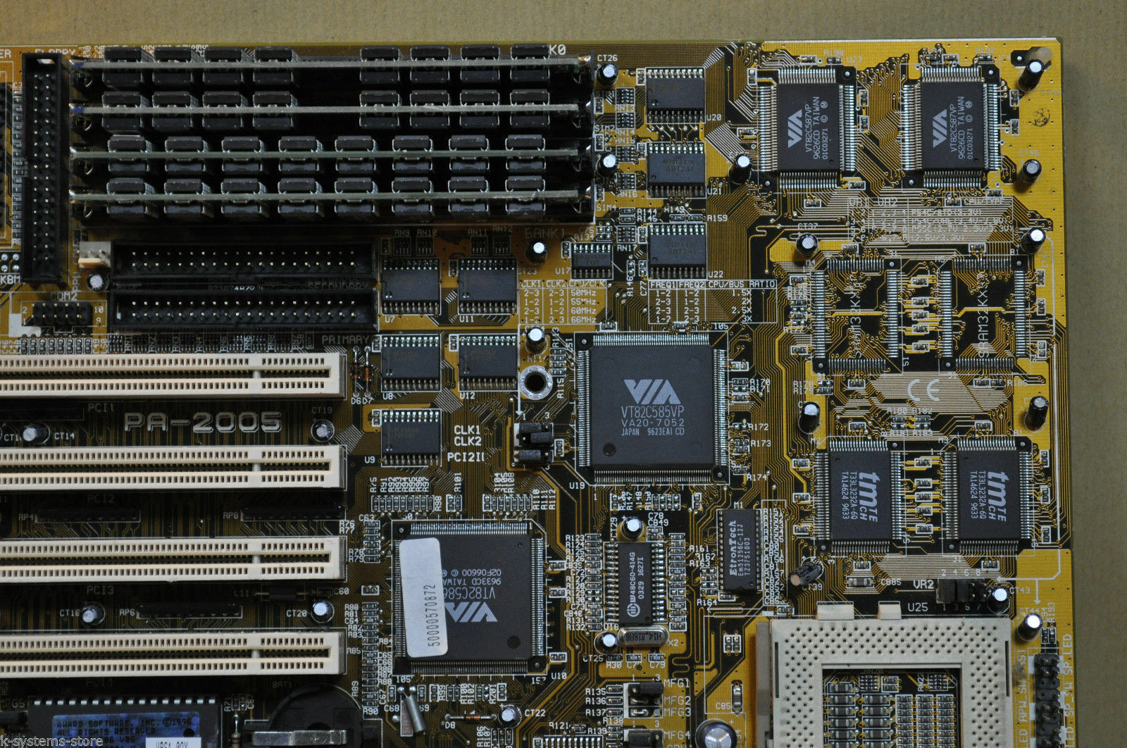
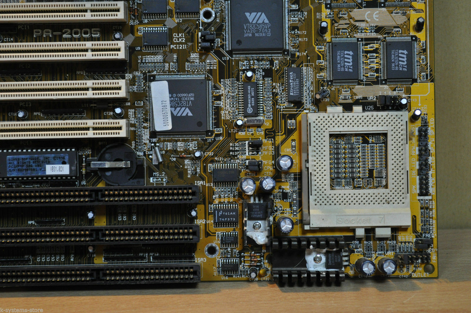
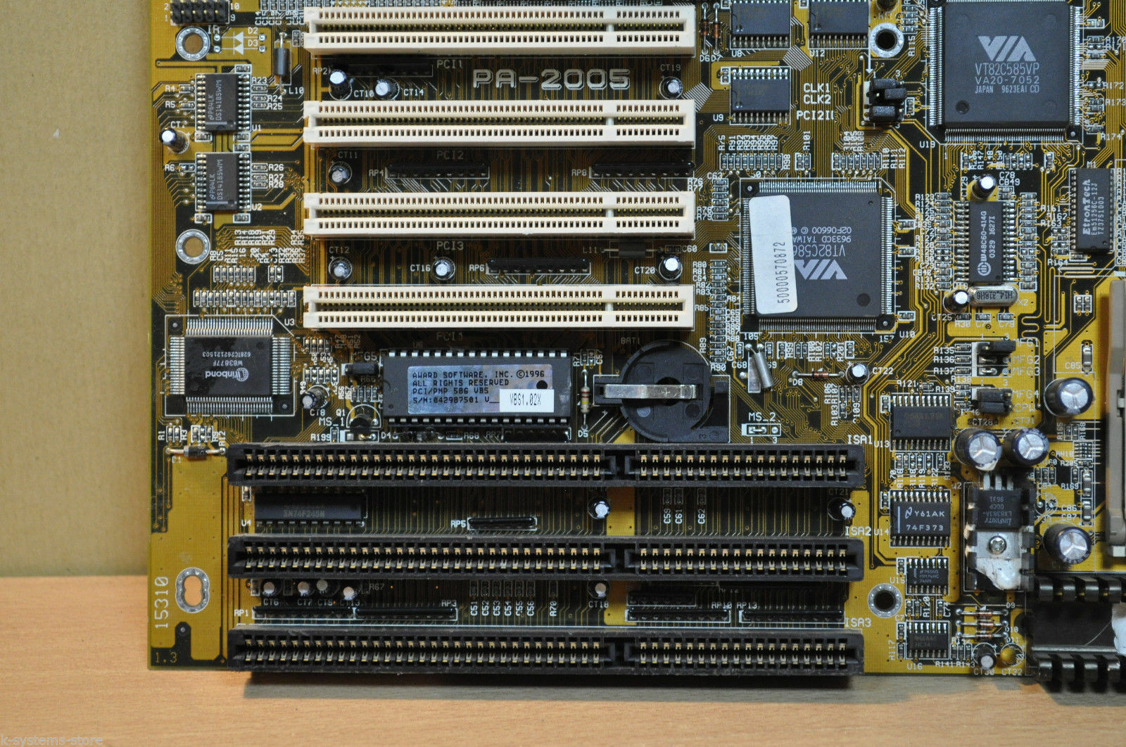
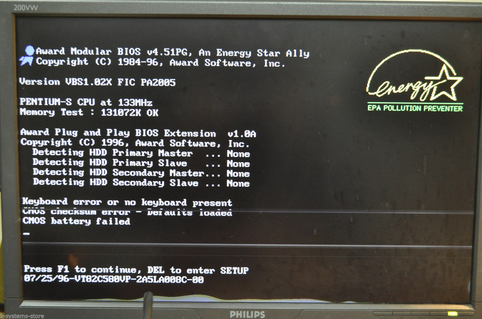
PA-2005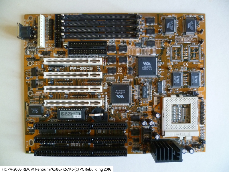
Year: 1997
Type: Socket 7
Form Factor: AT
Power Connector: AT
Chipset: VIA Apollo VP1
Slots: 3 x ISA (16-bit), 4 x PCI
Memory: 4 x 72-pin SIMM (2 banks), 512 MB max.
BIOS: Award 4.51PG
BIOS Dates: 05/07/96, 10/15/96
BIOS Strings:
10/15/96-VT82C580VP-2A5LA008C-00
Known Revisions: A.1
Supports bus speeds of 50 or 66 MHz. CPU clock speeds supported are 75-133 MHz (non-MMX). Revision A.1 is limited to a 66 MHz bus speed (jumper CLK3 is wired so it's not possible to set the bus at 75 MHz), but the final version (Apollo 585VP chipset) is certified to work at 75 MHz. With the 66MHz bus, the 1.5x clock multiplier is interpreted as 3.5x so you can also install Pentium MMX at 233MHz. Comes with 256 KB of Level 2 cache onboard.
CPUs Supported: Cyrix M1, AMD K5, Intel Pentium
CPU Clock Multipliers: 1.5x up to 3x.
The PA-2005 board supports the Cyrix 6x86 CPUs from P120+ to P166+.
User Manual
Addendum for AMD K6, Cyrix/IBM MX
Compatibility Test
Jumper Settings
BIOS Versions
BIOS Update 619J900 dated 08/21/97. Fixes system boot failure when using K6 CPU with 586_3028D, added new parting table for 6x86MX CPU.
More Images
PA-2006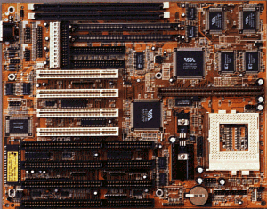
Year: ?
Type: Socket 7
Form Factor: Baby AT
Power Connector: AT
Chipset: VIA Apollo Master
Slots: 4 x ISA (16-bit), 4 x PCI
Memory: 2 x 72-pin SIMM (2 banks), 2 x DIMM (256 MB max.)
BIOS: Award 4.51PG
Known Revisions:
Supports Intel Pentium 75 - 200 MHz (MMX-ready), Cyrix/IBM 6x86 PR120+ - PR200+, AMD K5 PR75 - PR166.
Memory supported is EDO.
PA-2007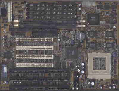
Year: 1997
Type: Super 7
Form Factor: AT
Chipset: VIA Apollo VP2
Slots: 3 x ISA, 4 x PCI
BIOS: Award
Memory: 4 x SIMM, 2 x DIMM
Known Revisions: 1.0
VIA Apollo VP2 chipset, 1 MB L2 Cache (2 banks), 2 DIMM/ 4 SIMM slots, 3 ISA / 4 PCI slots, good jumper descriptions, up to 75 MHz bus speed (no 83 sadly!), Award BIOS. Performance is excellent, especially under Windows NT although system sometimes doesn't boot if cache timing is set at 2 clock leadoff cycle (2-1-1-1); strangely using the 6x86MX at 75 MHz bus speed, it worked pefectly and amazingly fast thanks to the linear burst feature. You may have to select 3 clocks (3-1-1-1) to undergo the booting sequence with the K6 and the Pentium MMX with some BIOS revisions. I regret I was not able to get the 512 kB version in time for some comparison. Its performance should be around the same in this case (3-1-1-1). If you are a speed freak and need a cacheable area over 64 MB, take into consideration the PA-2007, it's one of the fastest boards at the moment for all configurations.
Does not support AMD K6-2+ or K6-III+ CPUs due to the lack of a low enough voltage selection (3.2V, 2.9V and 2.8V only).
PA-2010
Year: ?
Type: Socket 7
Form Factor: ?
Power Connector: ?
Chipset: ?
Slots: ? x ISA (16-bit), ? x PCI
Memory: ? x 72-pin SIMM (2 banks)
BIOS: Award 4.51PG
Known Revisions:
PA-2010+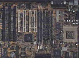
Year: 1997
Type: Super 7
Form Factor: ATX
Chipset: VIA Apollo VPX
Slots: 4 x ISA, 4 x PCI
BIOS: Award
Memory: 4 x SIMM, 2 x DIMM
Known Revisions: 4.0, 4.1
Here we have a VIA Apollo VPX chipset board in ATX format.
The K6 at 250 MHz was not identified correctly, but still worked fine. I had difficulties with the Pentium MMX 233. Sometimes it was detected as a Pentium MMX 133, but performance was good enough that I assume it was running at 233 MHz.
If you want to operate the motherboard at the fastest 83 MHz FSB, be aware you need the version with ICW W48C67-1 or ICS9147-01 clock generator - all others only support 75 MHz maximum. At 83 MHz bus speed, the SDRAM bank interleave had to be disabled, otherwise you will get lots of errors.
As with all VIA chipset-based boards, the PA-2010+ also supports the linear burst mode for Cyrix/IBM CPUs. With this you can expect performance gains of around 2-3%. If you are looking for an ATX board and VIA chipset, please consider the newer PA-2012 (1 MB) or the PA-2011 (with 512 kB) - they are much faster.
The PA-2010+ comes with 512 KB L2 cache onboard. External bus frequencies supported are 55, 60, 66, 75 and 83 MHz (the latter only possible with clock generator as described above). CPU core voltages supported are 3.2V, 2.9V and 2.8V only.
Other pictures: 1
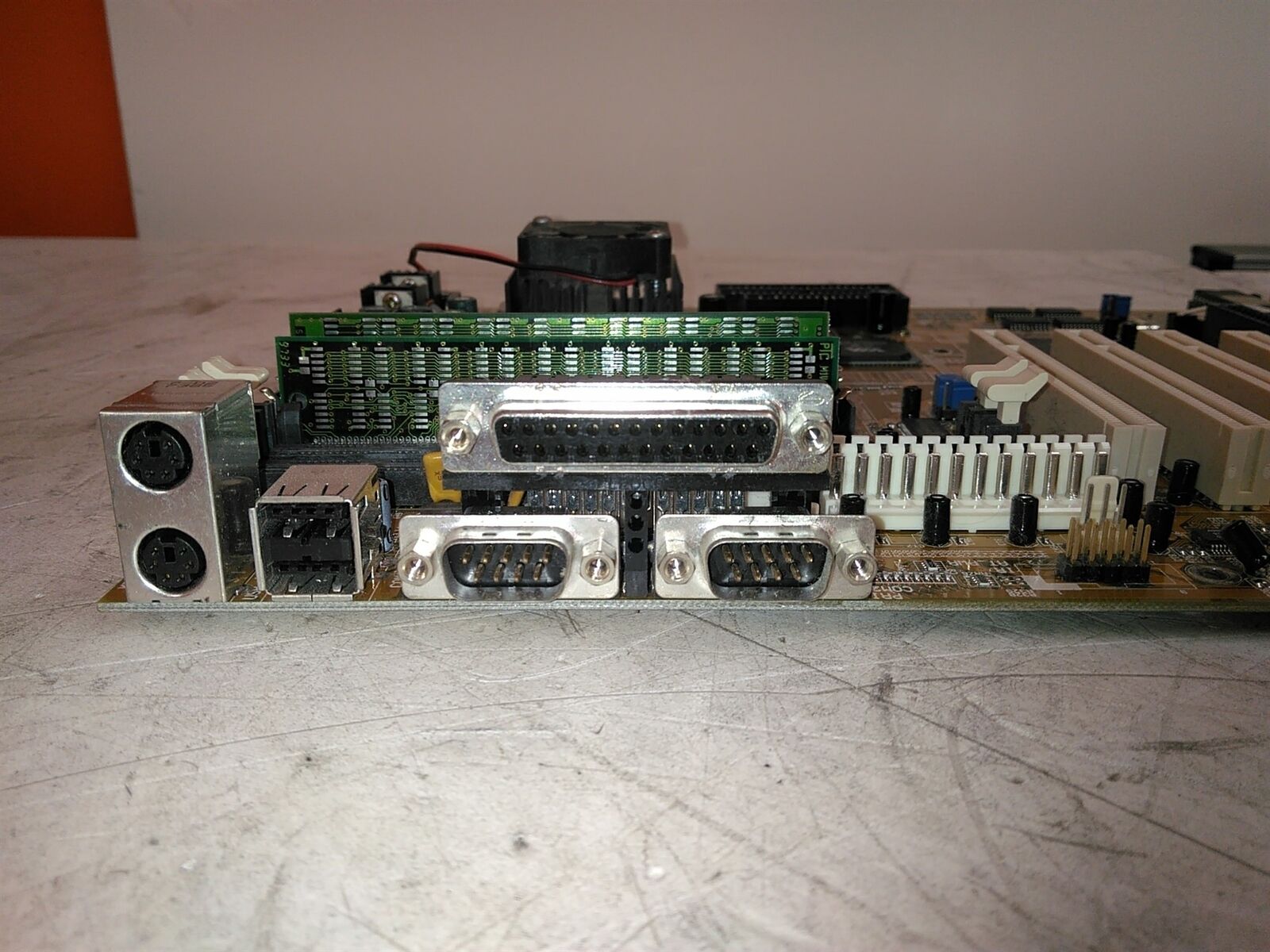
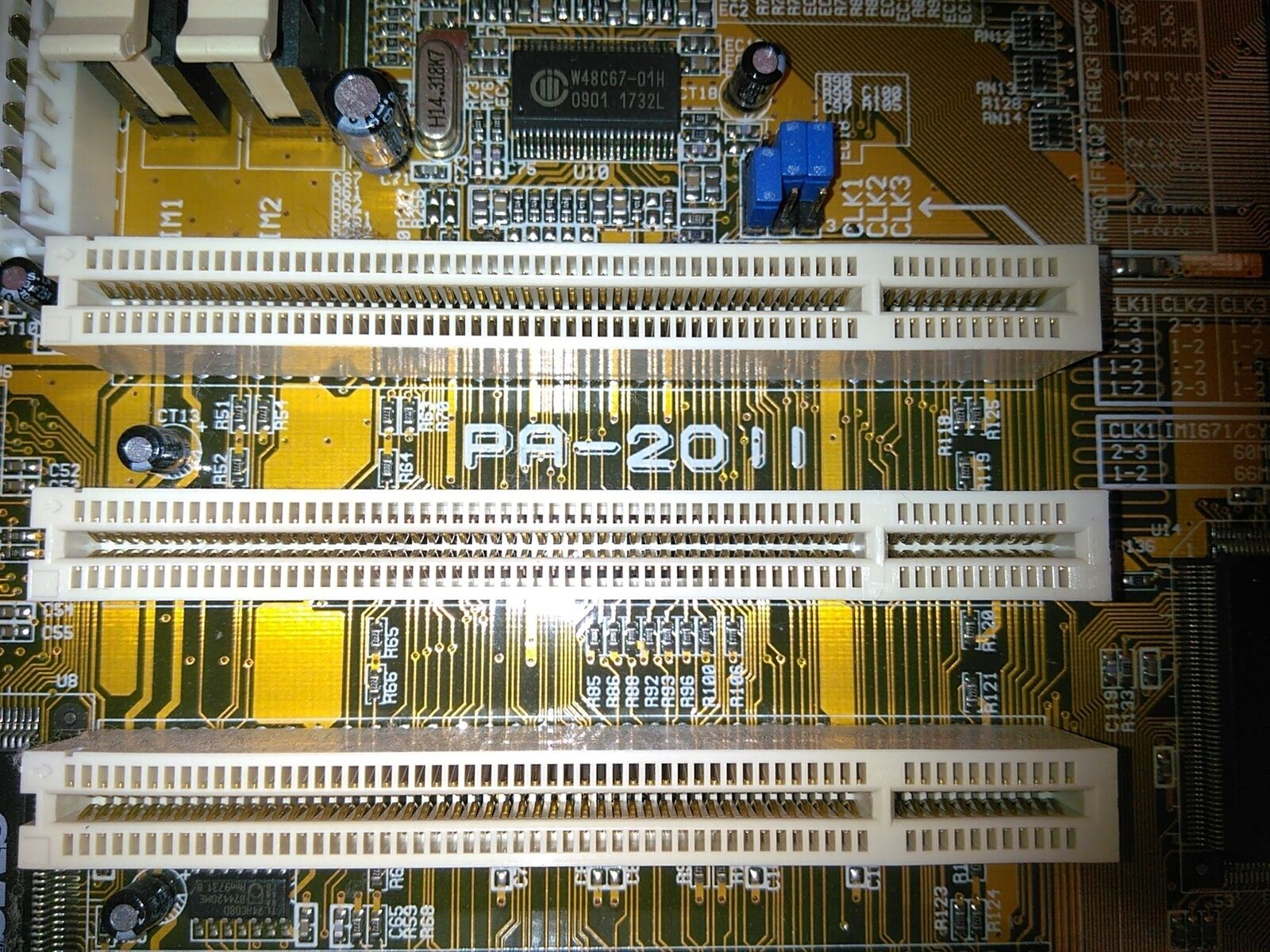
PA-2011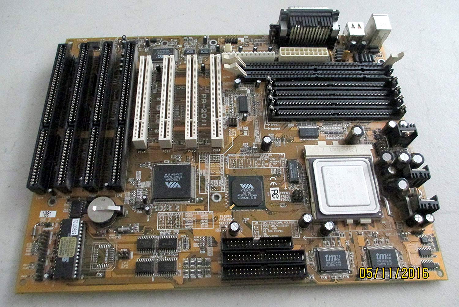
Year: 1997
Type: Super 7
Form Factor: ATX
Chipset: VIA Apollo VP2
Slots: 4 x ISA, 4 x PCI
BIOS: AMI
Memory: 4 x SIMM, 2 x DIMM
Known Revisions: 2.2
This is the ATX version of the PA-2007, but just with 512 KB of L2 cache. Technical facts are all the same.
Performance however, is not at the same high level as the PA-2007. The board has an additional connector for an AT power supply.
Our revision 2.2 does not have PCI special cycle support which the PA-2010+ has. The user gets into real trouble if he tries setting the SDRAM timing to 2/2 clocks. The result is that the board didn't want to talk with me until I made multiple use of the reset swich. I still haven't found out the reasons for this; it happened with every CPU and with EDOs instead of SDRAM, too. I'm confident a newer BIOS could improve this. I will also update this page as soon as I have some extra time to deal with this. Enable linear CPU burst when using Cyrix or IBM CPUs, you will be rewarded by a few per cents more performance. Be aware of using the Pentium MMX: This board is quite slow with it.
Supported bus frequencies: 50, 55, 60, 66, 75 MHz.
Core CPU voltages supported: 3.2V, 2.9V and 2.8V.
More Images
PA-2012
Year: 1997
Type: Super 7
Form Factor: ATX
Chipset: VIA Apollo VP3
Slots: 2 x ISA, 4 x PCI, 1 x AGP
BIOS: AMI
Memory: 3 x DIMM
Power Socket: 20-pin ATX
Known Revisions:
The FIC PA-2012 was the very first Socket 7 motherboard to support AGP.
Processors supported include the AMD K6 166 to 233 MHz, Intel P54CP55C, Cyrix 6x86 and M1 and M2. Clock multipliers of 1.5x, 2.0x, 2.5x and 3.0x are supported for P54C, 1x-4x for the Cyrix M1, and 2x up to 5.5x for the P55C, M2 and K6. Core voltage settings are 2.1V and 2.8V
Front Side Bus frequency settings are 55 MHz, 60 MHz, 66 MHz, and [on later board revisions] 75 MHz which drive the PCI bus at between 27.5 MHz to 37.5 MHz.
PA-2013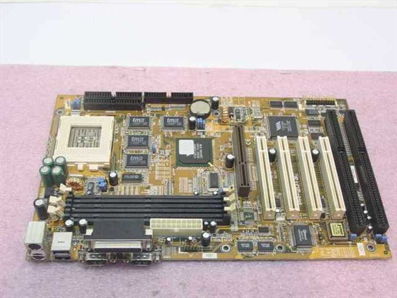
Year: 1997
Type: Super 7
Form Factor: ATX
Chipset: VIA MVP3
Slots: 2 ISA (16-bit), 1 AGP, 4 PCI
BIOS: Award
Memory: 168-pin DIMM
The FIC PA-2013 came with either 512 KB or 1 MB of level 2 cache on the board. The 2MB of L2 cache starts off by enabling the VIA MVP3 chipset's 508MB cacheable memory area, up from the 254MB of the 1MB version and the 127MB of the 512KB version.
Like all newer MVP3 based motherboards, the PA-2013 ships from the factory with revision 'CE' of the chipset which eliminates the problems the chipset had with i740 based graphics accelerators. The CE North Bridge is what drives the AGP 2X compliant port which is located just left of the chip itself.
This board does not support AMD K6-2+ or K6-III+ CPUs.
PA-2013 (2 MB cache)
Year: 1998
Type: Super 7
Form Factor: ATX
Chipset: VIA MVP3
Slots: 2 x ISA (16-bit), 1 xAGP, 4 x PCI
BIOS: Award
CPU Support: Pentium MMX, AMD K6-2, AMD K6-III, Cyrix MII
Memory: 168-pin DIMM
The FIC PA-2013 was a new generation of Super 7 motherboard, with support for AMD's K6-III processor. Since this CPU had its own L2 cache embedded on the CPU die, this bumped down the motherboard's "level 2" cache to be a "level 3" cache. The PA-2013 came with no less than 2 MB of this level 3 cache!
The board supports FSB speeds from 66 to 124 MHz, CPU clock multipliers from 1.5 - 5.5x, and CPU core voltages from 1.8V up to 3.5V in 0.1V increments.
The board also comes with two USB ports.
Like the original PA-2013, the 2MB version does come with Trend's ChipAway BIOS Virus Protection program that prevents boot sector viruses from loading even before your system starts up your operating system, just an added safety feature which may come in handy in this download-driven Internet world.
The PA-2013's performance rose an average of 3% in business applications, with performance increases peaking at the 5 - 7% level, placing it at the top of the Super7 motherboard performance charts. As you might be able to guess, the improvements in 3D games is virtually un-noticeable, so if you have a PA-2013 or another Super7 board right now that you're happy with, there is no point to upgrading to this 2MB version simply because of the performance increases. Even L2 cache dependent games such as Unreal didn't receive any improvement in performance as a result of the larger cache, in this case, their performance was being limited by the actual speed of the cache, not the size.
Memory support is via three 168-pin DIMM slots supporting EDO/SDRAM. Recommended RAM is PC100 SDRAM.
Now here's the real problem with that 2MB L2 cache, the board wasn't reliable enough at any overclocked FSB speeds (112MHz or 124MHz) most likely as a result of the quality of the L2 cache chips. Where the older PA-2013's outfitted with 512KB or 1MB of L2 cache could perform quite reliably at 112MHz, the 2MB version couldn't, making overclocking on this board, other than with the 100MHz FSB, undesirable.
A pretty good job as a board to stick a K6-3 on, but as for a K6-2 owner's overclocking wonder, the 2MB PA-2013 may end up being more of a disappointment.
PAK-2110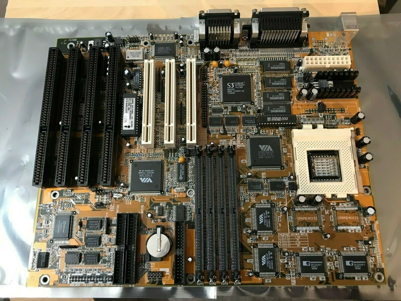
Year: ?
Type: Socket 7
Form Factor: AT
Power Connector: AT
Chipset: VIA Apollo VP1
Slots: 4 x ISA (16-bit), 3 x PCI
Memory: 4 x 72-pin SIMM (2 banks)
BIOS: Award 4.51PG
Known Revisions:
The PAK-2110 supports CPU multipliers of 1.5x, 2x, 2.5x and 3x. What makes it fairly unique for the era is the embedded S3 ViRGE video chipset.
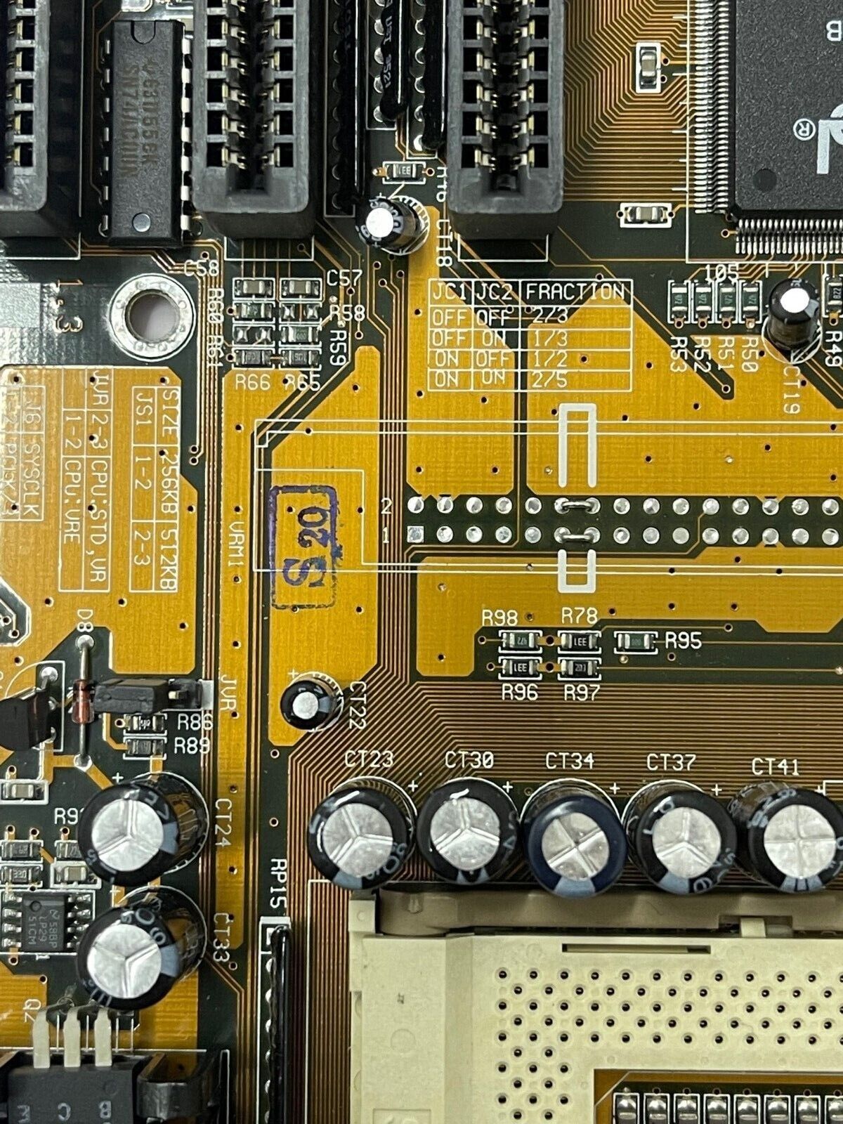
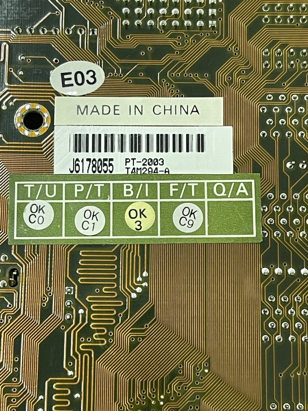
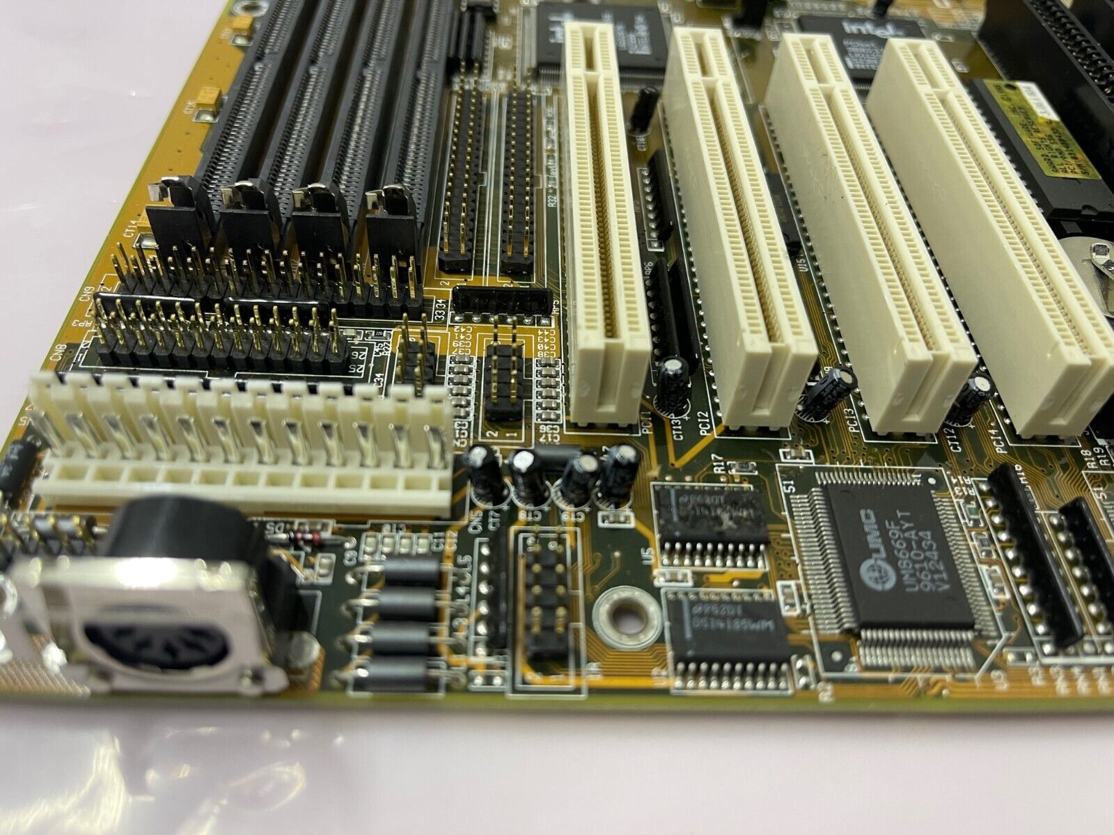
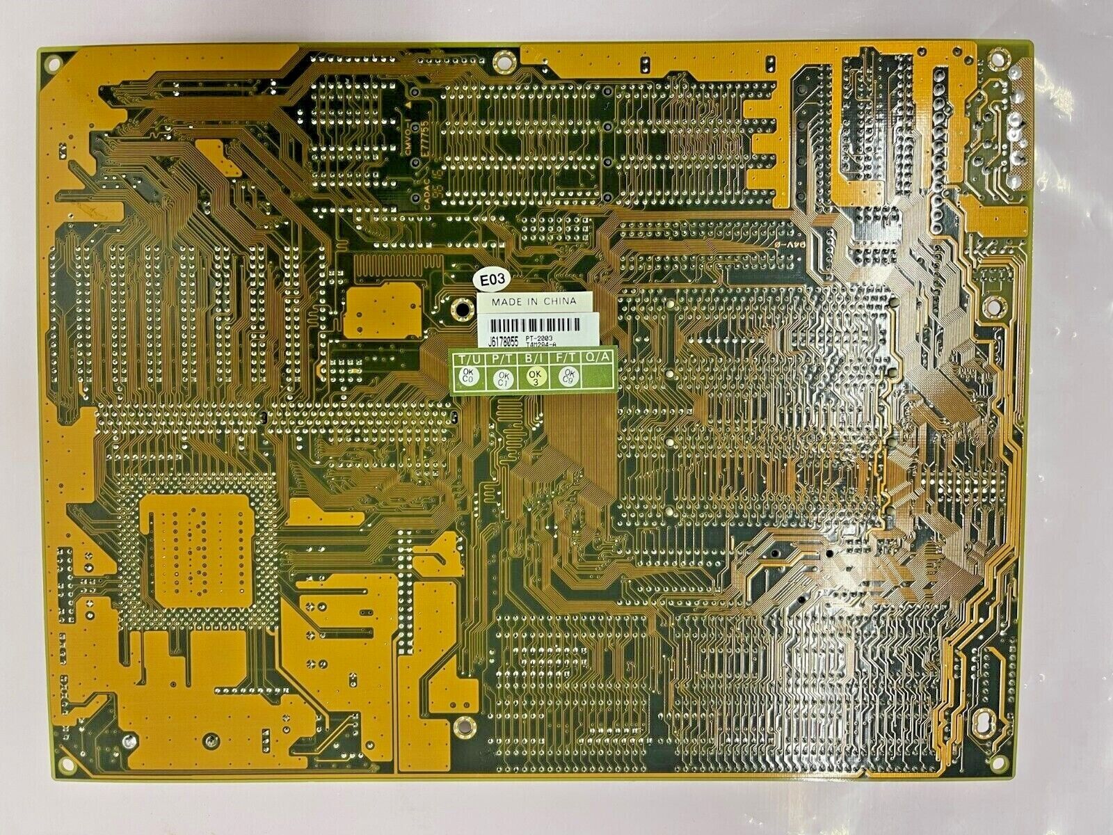
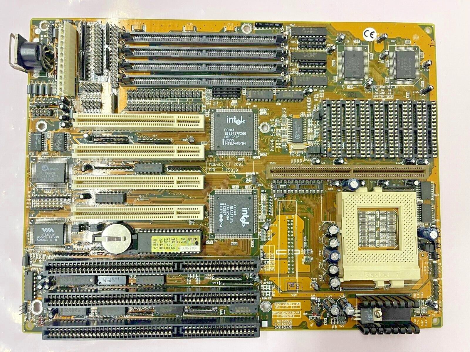 PT-2003
Year: 1995
Type: Socket 7
Form Factor: Baby AT
Power Connector: AT (P8/P9)
Chipset: Intel 430FX "Triton"
Slots: 3 x ISA (16-bit), 4 x PCI
Memory: 4 x 72-pin SIMM (2 banks)
BIOS: Award 4.51PG
Known Revisions:
More Images
PT-2006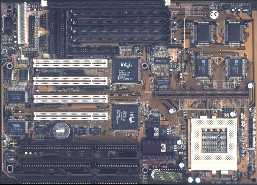
Year: ?
Type: Socket 7
Form Factor: AT
Power Connector: AT
Chipset: Intel 430VX "Triton 2"
Slots: 3 x ISA (16-bit), 4 x PCI
Memory: 4 x 72-pin SIMM (2 banks), 1 x DIMM
BIOS: Award 4.51PG
Known Revisions:
PT-2007
Year: 1997
Type: Super 7
Form Factor: AT
Chipset: Intel 430TX
Slots: 3 x ISA, 4 x PCI
BIOS: Award
Memory: 4 x SIMM, 2 x DIMM
Known Revisions: ?
This board has precisely the same layout as the PA-2007, the difference is the chipset. The PT-2007 is not suited for systems with more than 64 MB RAM due to the limitation of the cacheable area thanks to Intel's 430TX chipset. The BF2 jumper function has been integrated as well, but bus clocks over 66 MHz are not supported, FIC is strictly keeping the Intel specifications. I'm sorry I haven't had the time to try the remaining jumper setting possibilities, maybe 75 or even 83 MHz can be found. This will be updated as soon as I'll have time again to do this. Very hot: It's the second fastest board for the combination of Pentium MMX and Windows 95 and very fast with the K6 as well.
PT-2011
Year: ?
Type: Socket 7
Form Factor: ?
Power Connector: ?
Chipset: ?
Slots: ? x ISA (16-bit), ? x PCI
Memory: ? x 72-pin SIMM (2 banks)
BIOS: Award 4.51PG
Known Revisions:
PT-2012
Year: Nov 1997
Type: Socket 7
Form Factor: ?
Power Connector: ?
Chipset: VIA Apollo VP3
Slots: ? x ISA (16-bit), ? x PCI, 1 x AGP
Memory: ? x 72-pin SIMM (2 banks)
BIOS: Award 4.51PG
Known Revisions:
PT-2012 was the world's first Socket 7 motherboard to support AGP.
PT-2200
Year: ?
Type: Socket 7
Form Factor: ?
Power Connector: ?
Chipset: ?
Slots: ? x ISA (16-bit), ? x PCI
Memory: ? x 72-pin SIMM (2 banks)
BIOS: Award or AMI
BIOS Dates: Award 07/15/96, or AMI vTII v1.02
Known Revisions: 2.1
This board supports Cyrix 6x86 P120+ to P166+.
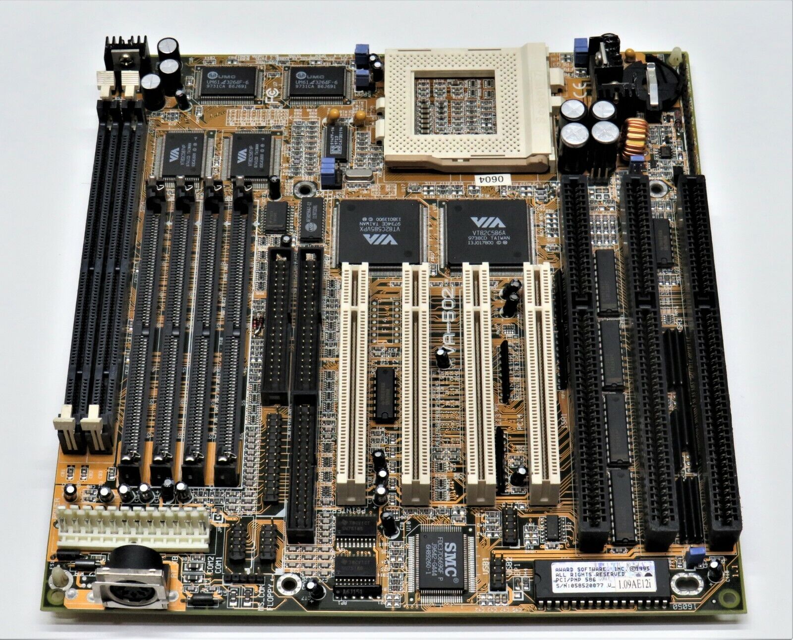
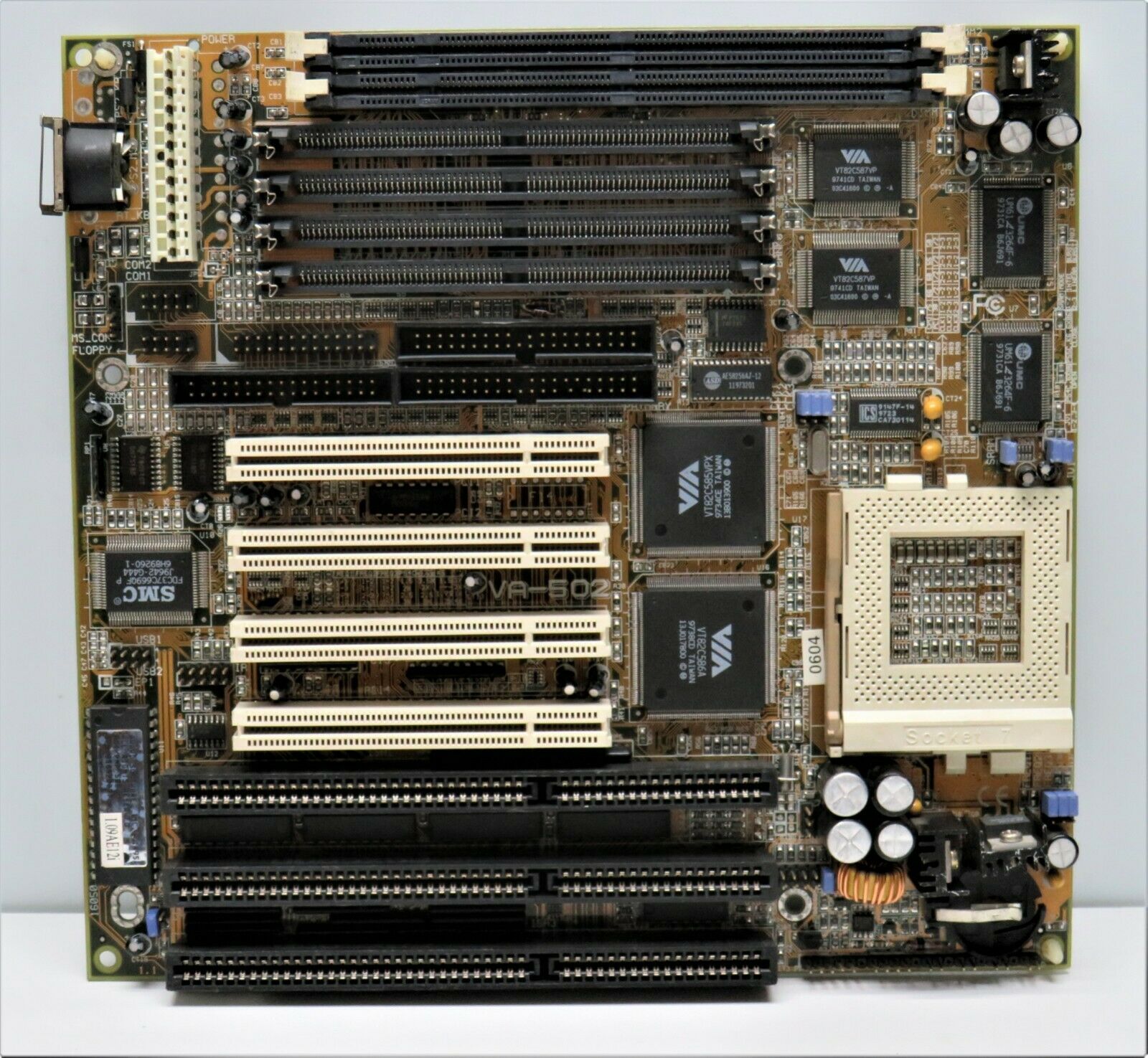
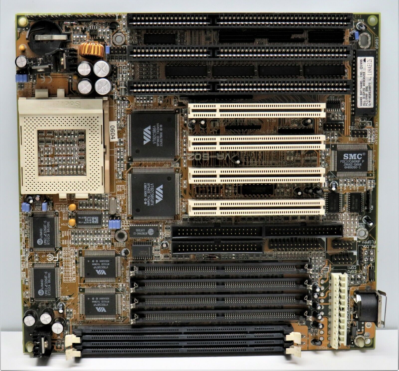
VA-502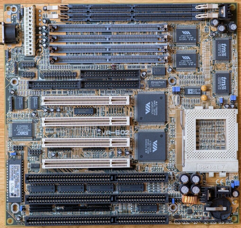
Year: 1997
Type: Socket 7
Form Factor: AT
Power Connector: AT
Chipset: VIA MVP3
Memory:
4 x 72-pin SIMM, 2 x 168-pin DIMM
Slots: 3 x ISA (16-bit), 4 x PCI
BIOS: Award v4.51PG
BIOS String:
05/28/97-VT82C580VP-2A5LA008C-00
More Images
VA-503
Year: 1997
Type: Socket 7
Form Factor: AT
Power Connector: AT
Chipset: VIA MVP3
Memory:
-
Slots: 3 x ISA (16-bit), 4 x PCI
BIOS: Award v4.51PG
BIOS String:
 VA-503+
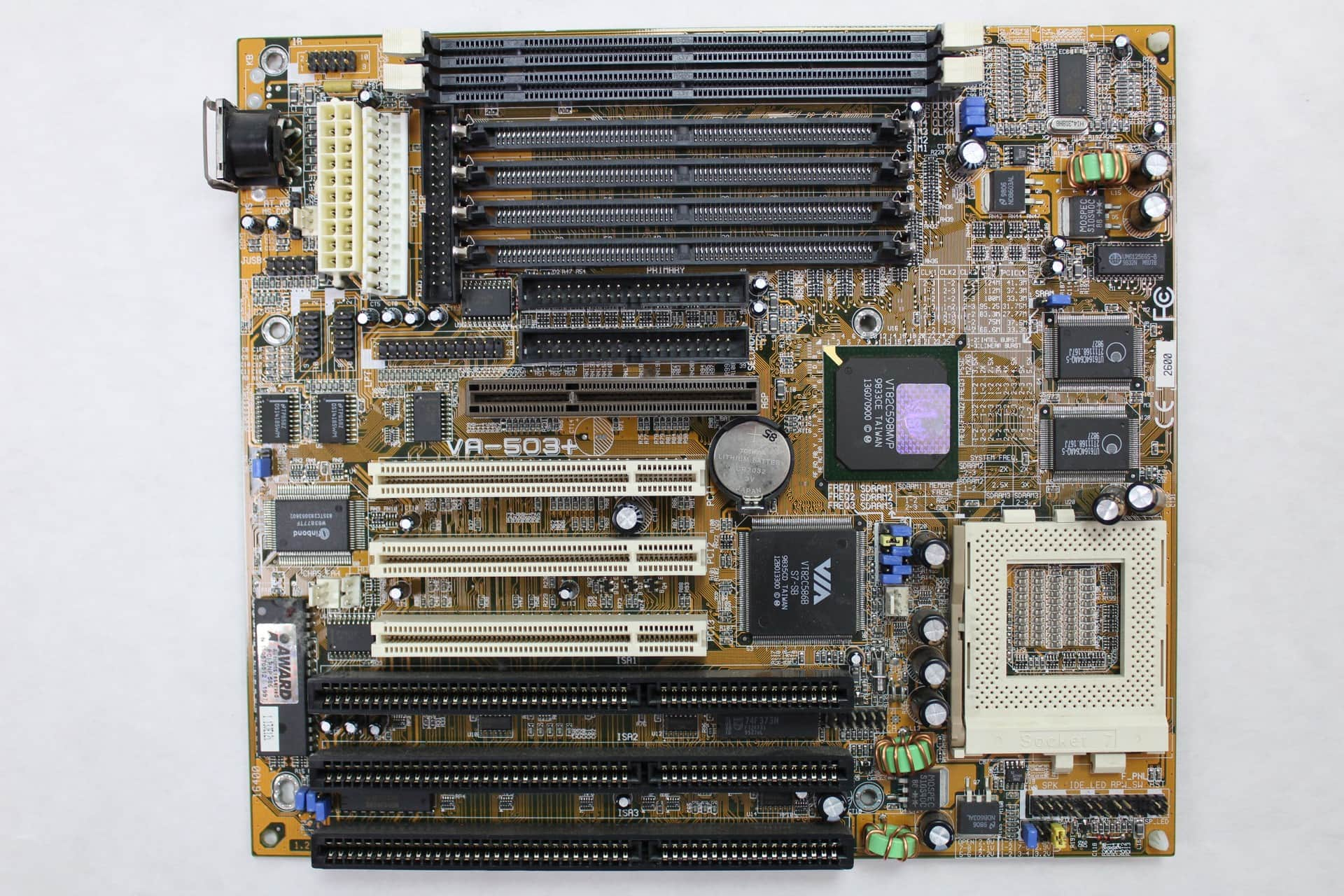
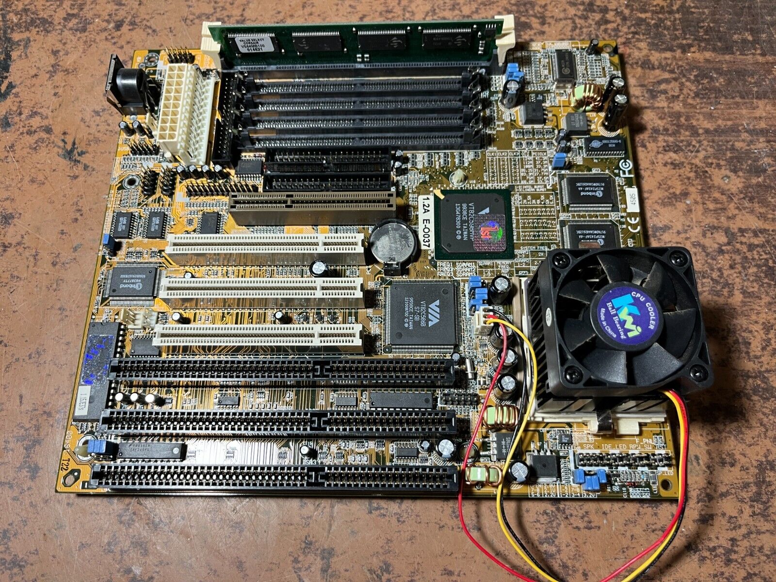
Year: 1998
Type: Socket 7
Form Factor: Baby AT
Chipset: VIA MVP3
Memory: 4 x 72-pin SIMM (EDO), 2 x 168-pin DIMM (for PC-66 or PC-100 memory)
Power Socket: AT (ATX
was added as a 2nd power option on a later board revision)
Slots: 3 x ISA (16-bit), 3 x PCI, 1 x AGP
BIOS: Award
Known Board Revisions: 1.0A, 1.1A, 1.2A
CPU support is broad: Intel, AMD and Cyrix processors are supported, and the Cyrix 6x86 MII Linear Burst Mode is available as a BIOS option. CPU voltage ranges are 2.0V up to 3.2V.
The VA-503+ supports FSB speeds of 60, 66, 75, 83, 95, 100, 112 and 124 MHz.
The board came with either a 512 KB or 1 MB L2 cache onboard with 5ns chips (necessary for MVP3-based boards to be stable at 100 MHz FSB or higher).
The AGP slot is AGP 2x, which is backward-compatible with AGP 1x.
A number of BIOS versions exist for the VA-503+. Those with 'JK' are designed for board revision 1.1A and those with 'JE' are designed for board revision 1.2A:
- 1.13JE11 - 25 May 1998 - no info on this BIOS version.
- 1.13JE12 - 3 Aug 1998 - no info on this BIOS version.
- 1.13JK10 - 4 Aug 1998 - no info on this BIOS version.
- 1.15JK31 - 19 Nov 1998 - added support for AMD K6-2 400MHz. For board revision 1.1A. Use the FIC utility FLASH625.EXE to flash this BIOS.
- 1.15JE32 - 2 Nov 1998 - adds CPU ID strings for Cyrix M(TM)II 450/400, K6(TM)-2 366/380/400, K6-3(TM) 400, Rise processor(s),fixed mismatch between IRQ routing table and miniport driver, and fixed SMBIOS table. For board revision 1.2A. Use the FIC utility FLASH625.EXE to flash this BIOS.
- 1.15JE33 - 19 Nov 1998 - added support for AMD K6-2 400MHz. For board revision 1.2A. Use the FIC utility FLASH625.EXE to flash this BIOS.
- 1.15JK34 - 22 May 1999 - adds support for 95 MHz, AMD K6-2 and K6-3+ CPUs, and ATA/66. For board revision 1.1x. Use the FIC utility FLASH703.EXE to flash this BIOS.
- 1.15JK35 -26 Aug 1999 - no info on what this version fixes/adds. For board revision 1.1A. Use the FIC utility FLASH73.EXE to flash this BIOS.
- 1.15JE36 - 22 May 1999 - adds support for 95 MHz, AMD K6-2 and K6-3+ CPUs, and ATA/66. For board revision 1.2A. Use the FIC utility FLASH703.EXE to flash this BIOS.
- 1.15JE37 - 19 Aug 1999 - no info on what this version fixes/adds. For board revision 1.2A. Use the FIC utility FLASH73.EXE to flash this BIOS.
- 1.15JE438 -7 Apr 2000 - adds support for AMD K6-2 550MHz CPU. For board revision 1.2A. Use the FIC utility FLASH73.EXE to flash this BIOS.
- 1.15JE439 - 26 May 2000 - fixed COM port mouse can't work under WIN98 ACPI mode. For board revision 1.2A. Use the FIC utility FLASH73.EXE to flash this BIOS.
More Images
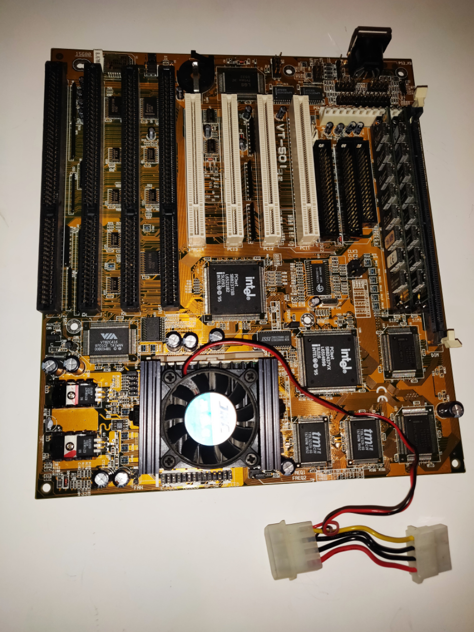 VT-501
Year: ?
Type: Socket 7
Form Factor: AT
Chipset: Intel 430VX "Triton 2"
Memory: 2 x 72-pin SIMMs, 1 x 168-pin DIMM
Slots: 4 x ISA (16-bit), 4 x PCI
BIOS: Award v4.51PG
BIOS String: 04/02/97-i430VX-2A59GF0bC-00
Known Board Revisions: 1.1