Can I Get a 286 To Run Like a 386 - Part 2
16th October 2021
In Part 1, I took a look at the Harris 80286-25 along with the fastest 286 chipsets produced, and observed some synthetic benchmarks that others have taken in the past.
In this part 2, let's take a look at the LM103S 80286 motherboard that just arrived and do some tests on it in stock form.
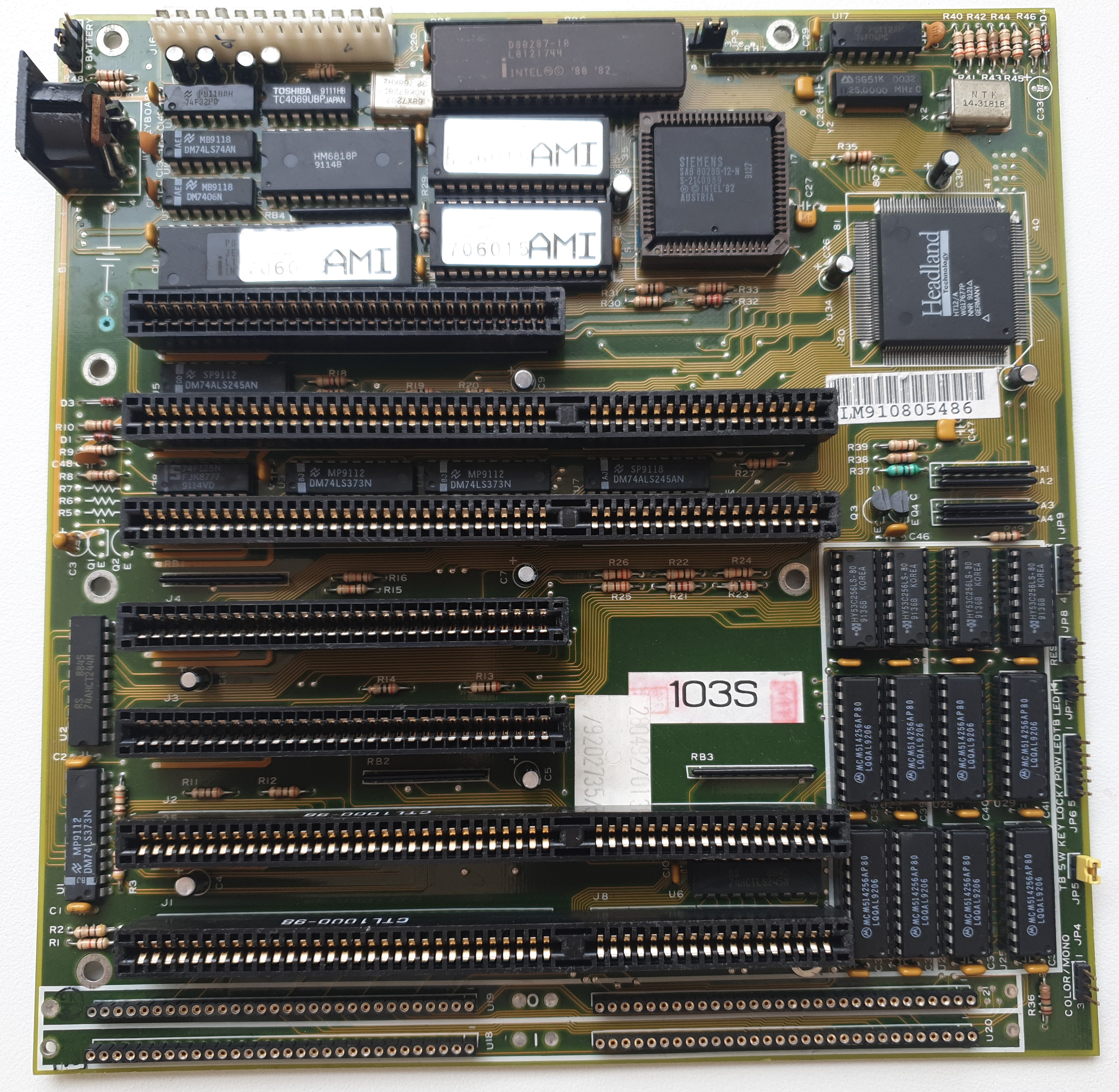
The LM103S - won on Ebay for about £27 plus taxes
What drew me to this particular Baby AT board is the socketed 286 in addition to the single-chip Headland chipset. The board is missing the CMOS backup battery - probably a Varta barrel type which many of us now know were very prone to leakage - some corrosion is still evident which will need to be cleaned up. The board has no identifying marks on the silkscreen to indicate its manufacturer or model number but does have a few stickers that lead me to thinking it's some variant of the LM-103S. What is slightly odd is the 2-chip BIOS with a label dated 1986, while other ICs on the board are dated 1992 - that's quite a date range! Searching through Stason.org and other online searches reinforced my belief that this is indeed an LM-103, of sorts. I could not find a picture of an LM103 (no 'S') anywhere to confirm, so I may be way off base - if you can help me identify my board, please get in touch!
Quick Visual Inspection
As I tend to do with my motherboard reviews, let's do a fly-by to see what we have:
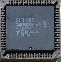
- A socketed Siemens-branded 80286-12.
- Headland HT12/A single-chip chipset (Headland Technologies).
- A socketed Intel 80287-10 math co-processor.
- Two AMI BIOS chips (high and low).
- An American Megatrends keyboard BIOS.
- Twelve 256 Kbit DRAMs for main memory, and two rows of sockets at the bottom that are SIPP headers.
- Four 16-bit ISA expansion slots and three 8-bit.
- AT P8/P9 power connector
- Full-size DIN keyboard socket
Date-wise, the most recent date stamp on the motherboards' non-socketed chips is week 21 of 1991 (the HT12/A chip), so it was certainly no earlier than mid-May 1991 when this was originally manufactured. Having said that, if the DRAMs have not been replaced, the latest date code is week 6 of 1992.
The Component Parts
The CPU
 The 80286 CPU started off in clock speeds of 4, 6 and 8 MHz. Intel's versions of these later went up to 12.5 MHz, of which this is one. It is probably the most common 286 speed that was sold, as it sat firmly between the fastest XTs and the low-end 80386 PCs.
80286s were usually manufactured in an "LCC" (Leadless Chip Carrier) package, either in Ceramic (CLCC) or plastic (PLCC) form. Rather than other ICs which have "leads" (pins), these have rounded pins underneath that compress when they go into the socket, supposedly to reduce the risk of bending a pin during insertion or extraction. They are still a real pain to get out of their socket, especially if they've been in there for 30 years! The best way to remove the CPU is to use a dedicated IC puller which comprises two prongs that fit into the two opposite corners. You can then pull up whilst rocking the CPU from side to side.
This LM-103S motherboard has three crystal oscillators: A 32.768 KHz one, another that is 14.31818 MHz, and a third which is a Seiko-Epson one in a 4-pin package and rated at 25.0000 MHz. The latter here is for the CPU with a CLK/2 setting, so is perfect for running the 12 MHz CPU. The 32 KHz one is most likely for keyboard timing, and the 14.31818 one would be for the FPU or the AT bus (again, at CLK/2).
The Chipset
The chipset found on this board is my main reason for the acquisiton - it's the popular Headland HT12/A PC/AT chipset which was released in August 1990, and is known to be very stable and reliable.
The HT12/A is supposed to be capable of driving 80286 processors up to 20 MHz with an appropriate crystal oscillator to match, so it will be interesting to see if I can upgrade this board and finally test my Harris 80286-25 which has been lying around for over a year untested.
Memory
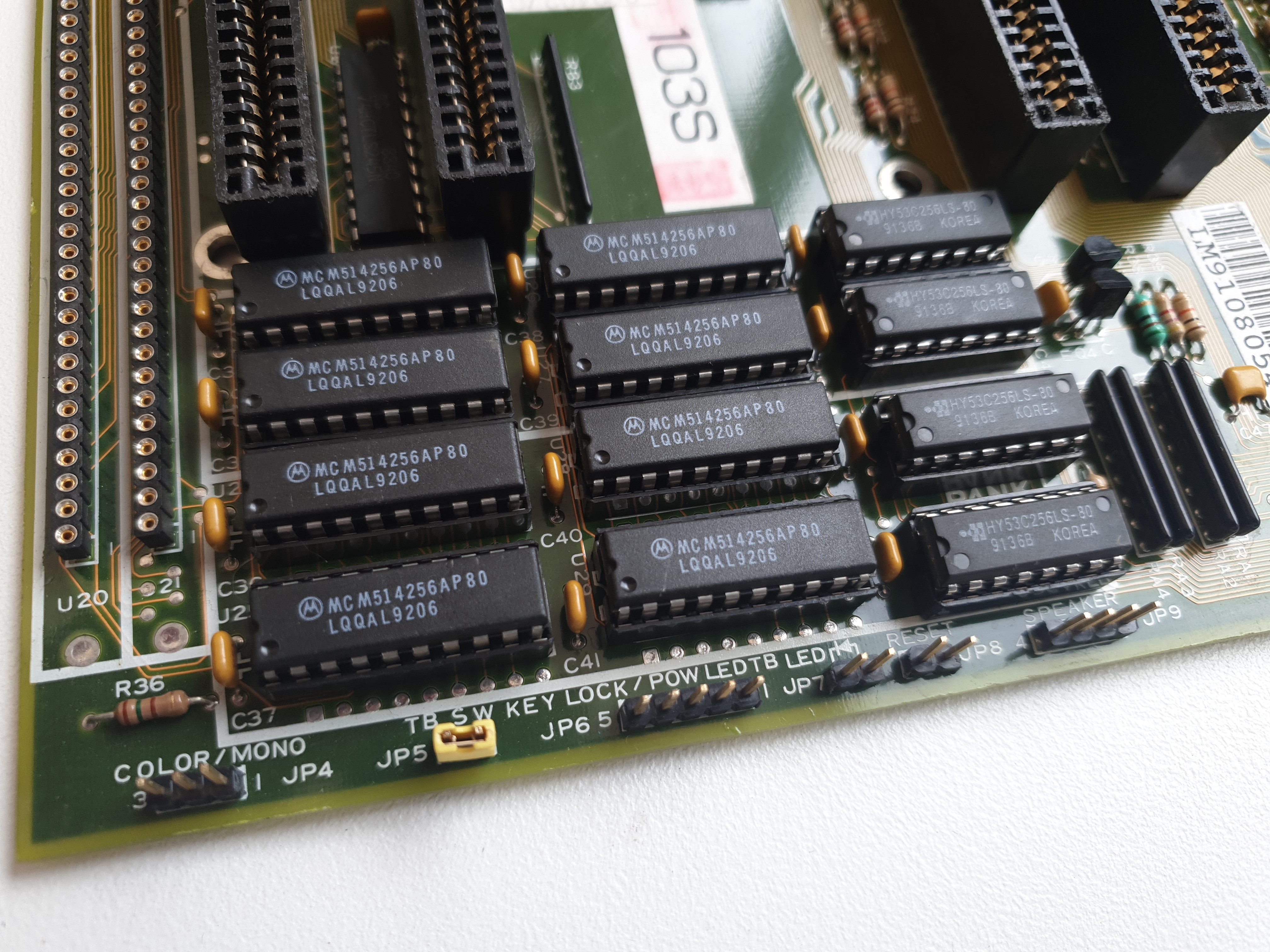 The motherboard has twelve DRAM sockets, populated with a mix of 256K x 4 and 256K x 1 memory chips. These appear to be in two banks with the upper six chips being 'Bank 0' and the lower six being 'Bank 1'.
It supports a maximum of 4 MB of memory if 1 Mbit DRAM chips are used - this is very common even on high-end 80286 motherboards, as 4 MB is plenty for typical tasks these PCs would have been doing in 1991. Despite the fact that the 80286 can address up to 16 MB over its 24-bit address bus, motherboard support for a full 16 MB was quite rare. Since this board has 256Kx4 chips, it has 1 MB of memory onboard.
All 12 DRAM memory chips are 80ns. While this rating might be fine for a 12 MHz 80286, it will certainly be insufficient to run the board with zero wait states at higher frequencies like 20 MHz. I will see if I can get some 60ns ones, either in DIP form or SIMM/SIPP.
The SIPP slots are one of the negative aspects of this board - great that we have a means of memory expansion, but SIPPs weren't around for very long, and these days are very rare/almost impossible to buy cheaply.
Jumpers
This 286 motherboard has no jumpers or DIP switches.
Other test hardware
For video, as I've done before, I made use of my excellent Cirrus Logic CL-GD510/520 auto-switching Super VGA card. It's not fast but it continues to be extremely reliable, and as I think I've mentioned a few times, I just love the text font on this card! Plus it's very "period correct" as it dates back to 1989 - it would have been a perfect option for this PC back then.
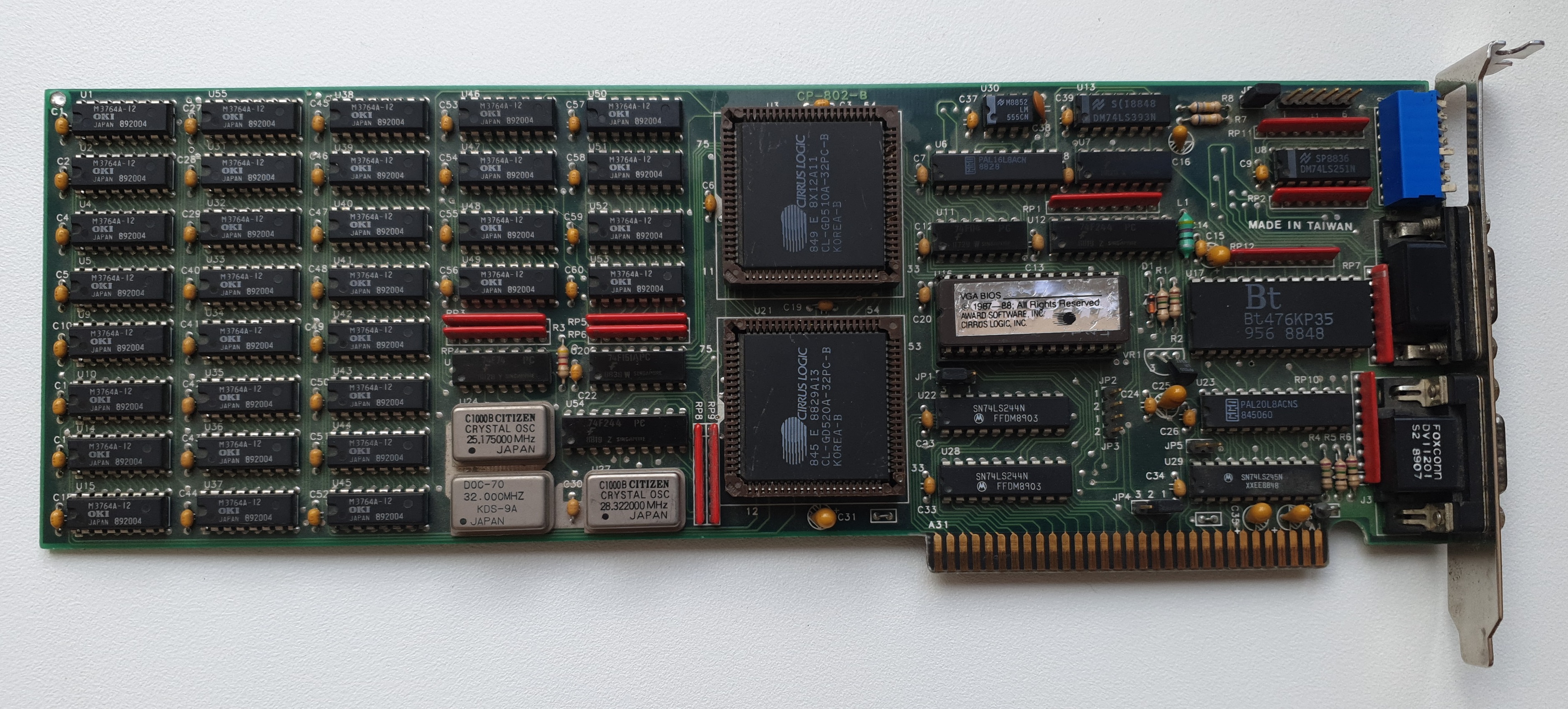
My Cirrus Logic CL-GD510/520 Super VGA video card with Eagle II BIOS
For power, I will use an ATX 400W PSU from an old Pentium 4, coupled with an ATX-to-AT adapter, and my trusty IBM 101-key enhanced PS/2 keyboard with a PS/2-to-DIN adapter.
POWER UP!
The board was bought as 'Used but fully working'. I powered it up and...
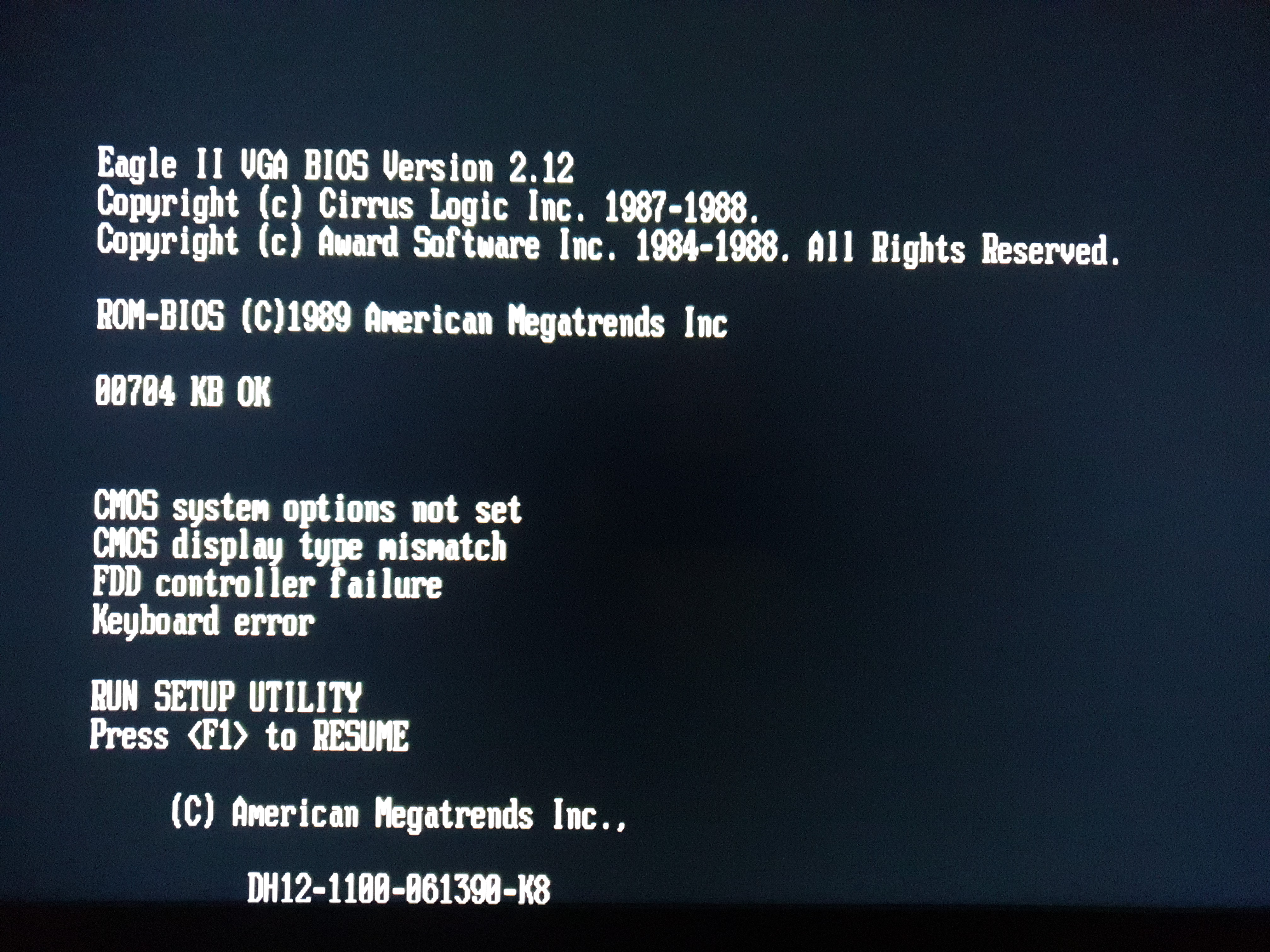
It's alive! (always a bit touch and go with hardware that is 30 years old)
The RAM reading up to 704 KB is interesting - my guess is some is being used for ROM shadowing (the moving of ROM code into faster RAM for speedier BIOS calls). The BIOS string at the bottom of the screen, DH12-1100-061390-K8 tells me this is a Taiwanese board, but the 100 is not a known AMI customer ID - it is likely the BIOS version, not a manufacturer code. The 061390 tells us the BIOS date is 13th June 1990, and a keyboard BIOS version 8.
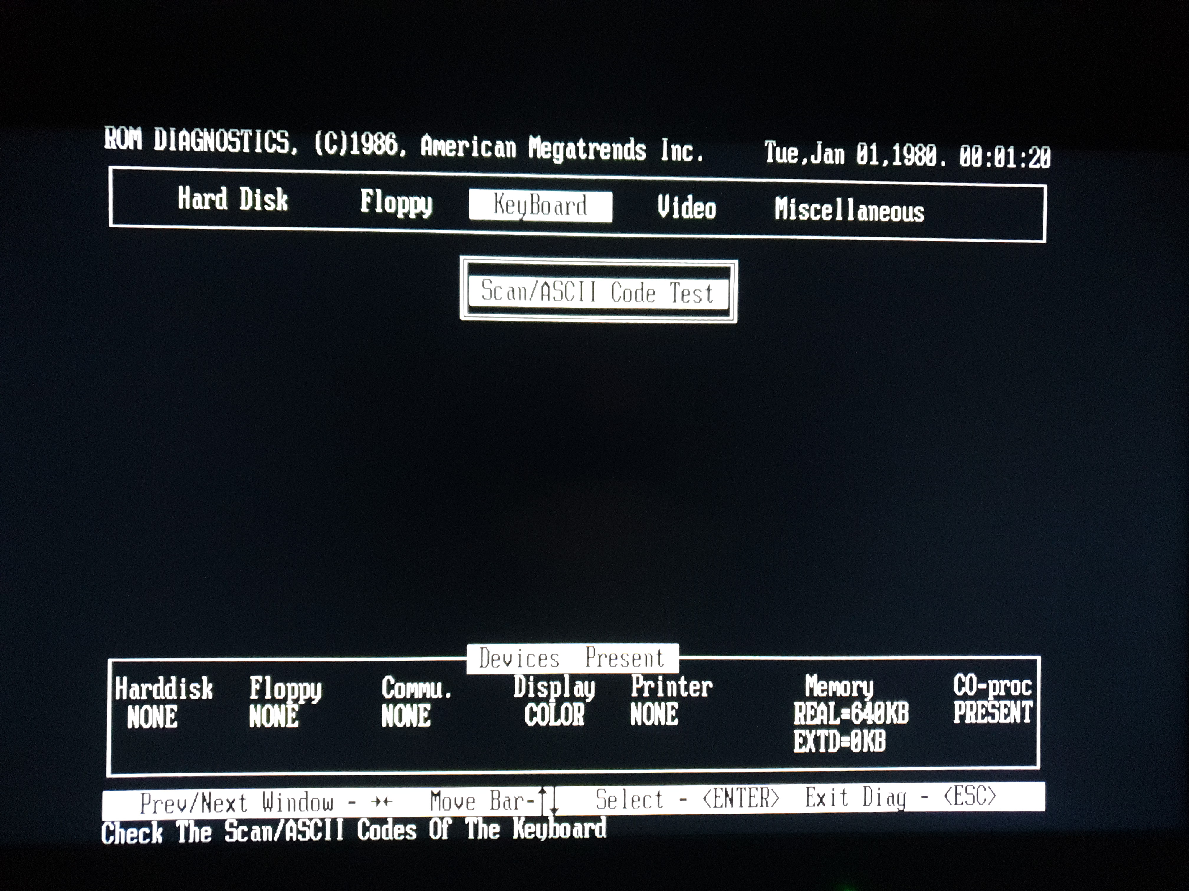
Here are all the pics of the BIOS setting screens:
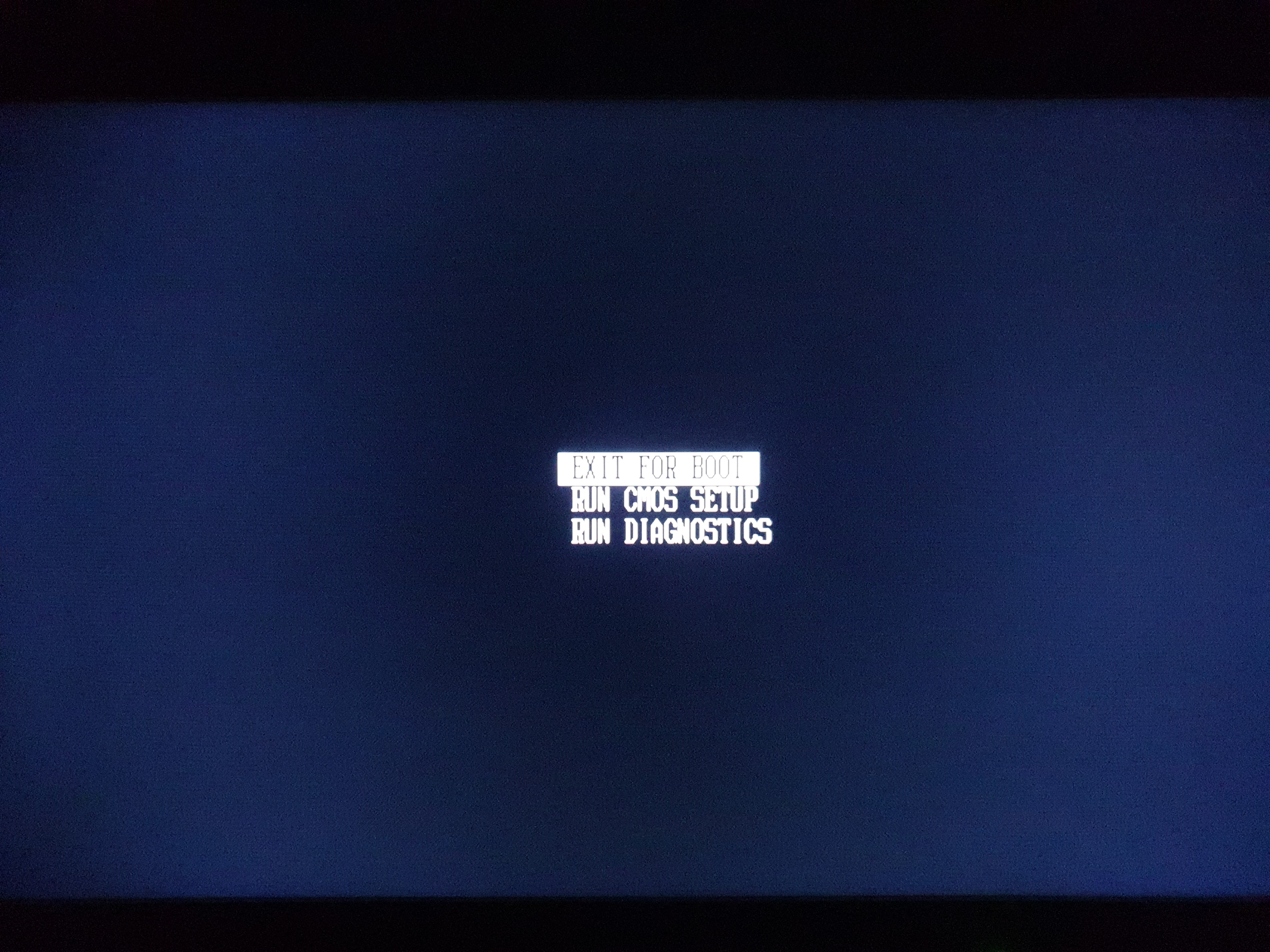
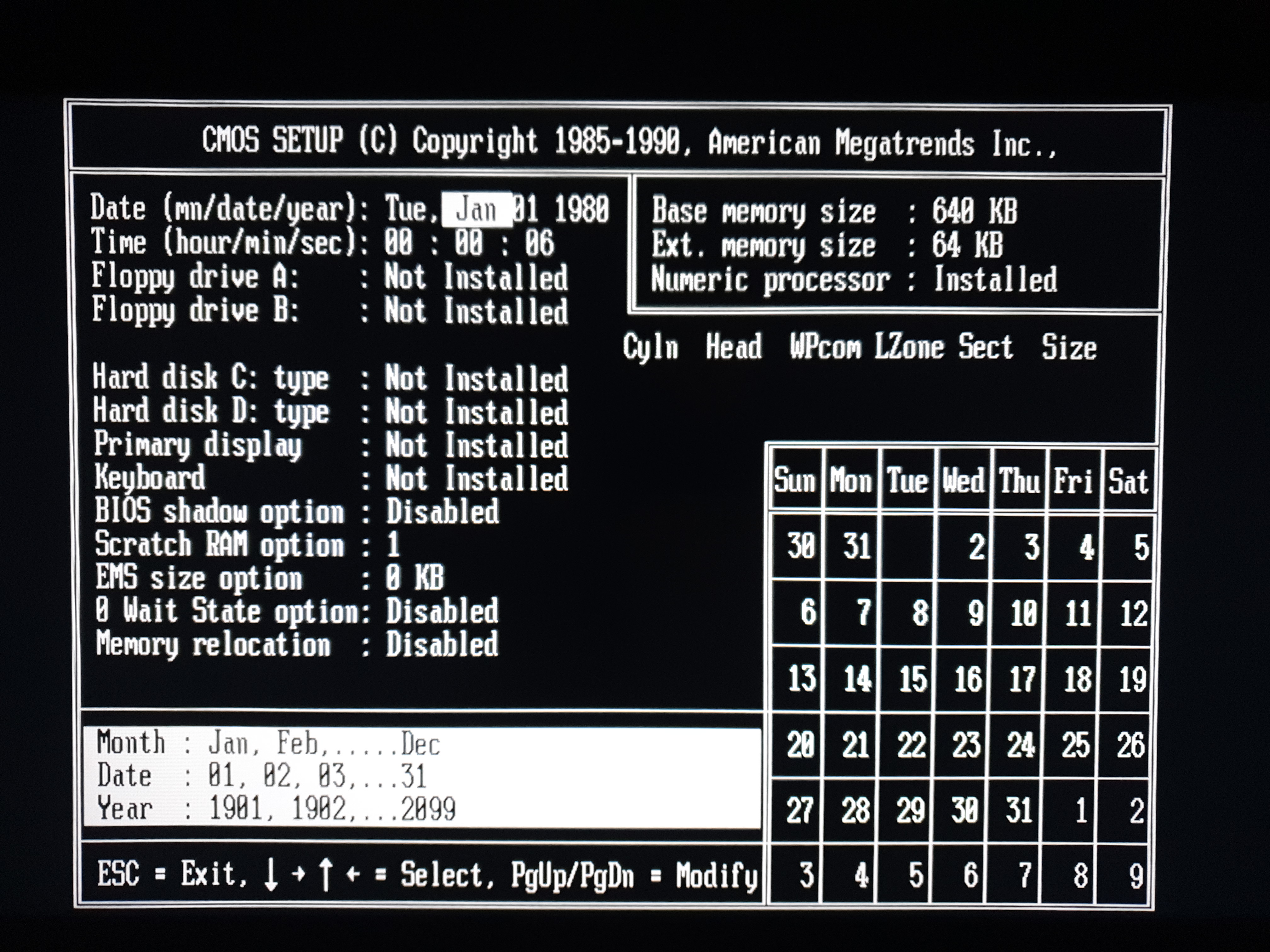
From left: (1) initial options when you press <DEL> on startup, (2) the 'CMOS Setup' page,
(3) the 'Run Diagnostics' page
So it's pretty basic really - very similar to my early C&T 386 board's AMI BIOS of similar vintage, except this has far fewer options.
The diagnostics screen doesn't allow you to go to the 'Hard Disk' or 'Floppy' menus unless these are configured on the CMOS Setup screen. Under 'Video' you can run some tests to ensure video modes are working as expected. Under 'Miscellaneous' you can test any serial or parallel ports that have been detected.
In Part 3, I'll get a hard disk wired up, get it booting to a DOS prompt, and then run some benchmarks on the board in its stock form.