Retro Review: UMC VGA Card Part 1
29th June 2026
I dug out another 16-bit ISA VGA card for review today, and it's one I know nothing about. Based on the UMC UM85C408AF chip, this dates to mid-1994. A quick search of the card's FCC ID told me this is from United Microelectronics Corporation (UMC) themselves! Will it be a diamond or a dud? Let's find out...
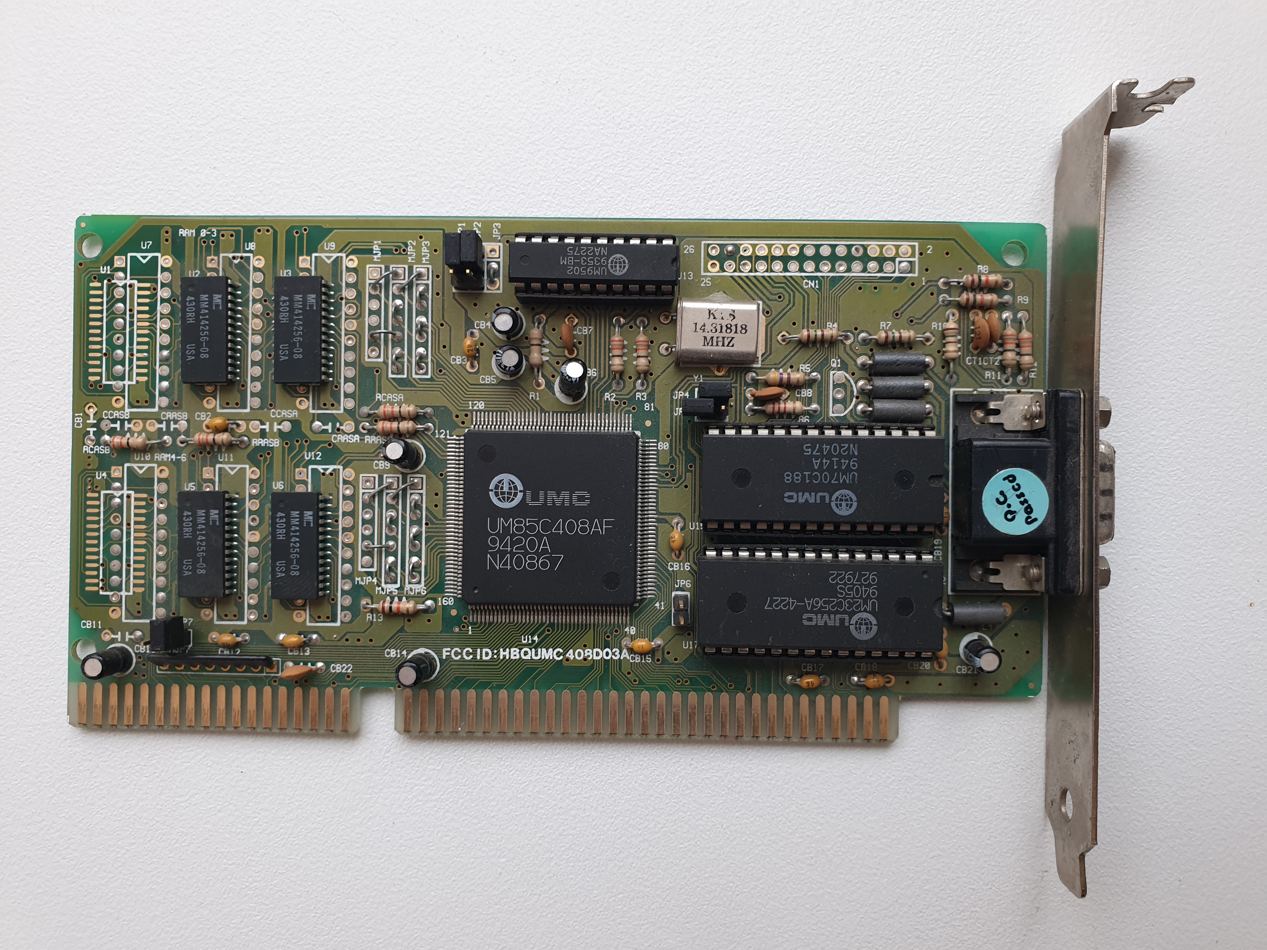
The UMC 16-bit ISA card (ca. 1994)
UMC were more commonly known as a motherboard chipset and CPU manufacturer, mostly during the Socket 5 486 period - certainly not well known for their graphics cards.
The Flypast
So what component parts make up this little 16-bit ISA graphics card? It appears to have:
- A UMC UM85C408AF video chipset
- A UMC VGA BIOS chip (UM23C256A)
- A UMC RAMDAC (UM70C178)
- A UMC clock generator chip (UM9502)
- A single crystal oscillator
- A 15-pin D-SUB for analogue video out
- Four DRAM chips, each 128KB in size
- Six jumpers (three of which have pin headers)
Video Controller
The UMC UM85C408AF datasheet is nowhere to be found, but it appears this VGA chipset was able to access up to 1 MB of video memory.
It was also apparently able to support up to 75 Hz vertical refresh rates and screen resolutions up to 1024 x 768.
Around the time of this UM85C408, there was a more premium 32-bit VESA Local Bus chipset with a built-in IDE controller called the UM85C418, and a little before the 408 they had the UM85C405.
You can read a discussion on Vogons around the relationship between this UMC chipset and the Genoa GVGA (GN007001-B). It's understood that this UMC 408 was based on the GVGA, but there are distinct differences. The Genoa chip can only access 512 KB of memory (3 bits used to address the bank) where the UMC uses 4 bits to address the bank, i.e. 1 MB addressable.
It's possible the earlier 405 was a clone of the GVGA chip and the 408 was closer to the 418 in terms of how it can access 1 MB but did so that was incompatible with the GVGA. 408 low-level code works 100% with the 418.
The UM85C408 was also used on the Gainward Cardex V1-1AV VESA Local Bus VGA card (though usually they used the 418) which reinforces to this assumption.
VGA BIOS
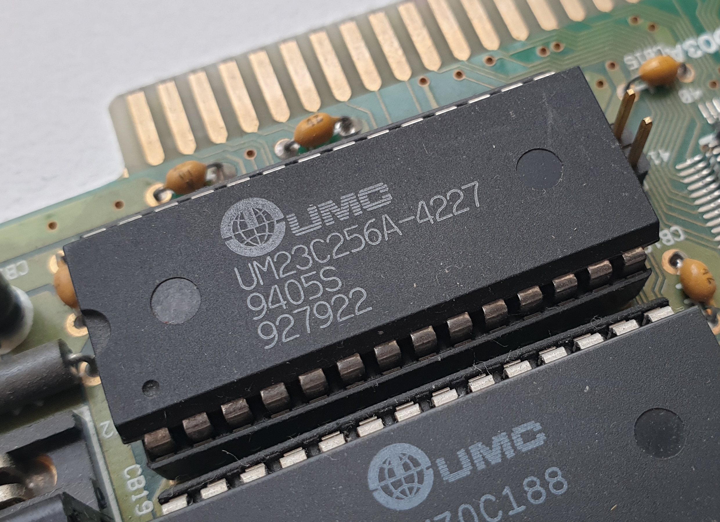 The Super VGA BIOS is a 28-pin 27256A-equivalent EPROM chip (256-kbit), which means it's 32 KB in capacity. I have taken a dump of the ROM using an EEPROM reader (NEC UPD7C256A is correct identity for this IC) - you can download it here.
The BIOS string looks like this:
**** UMC SuperVGA UM85C408 70Hz - 1991, 1992 **** BIOS VERSION: 1.04, BOARD VERSION ISA-1AV DATA: DRAM: 256K DRAM: 512K DRAM: 1M 09/29/93 (C) COPYRIGHT AWARD SOFTWARE, INC. 1991(C) COPYRIGHT UNITED MICRO CORP. 1989RAMDAC
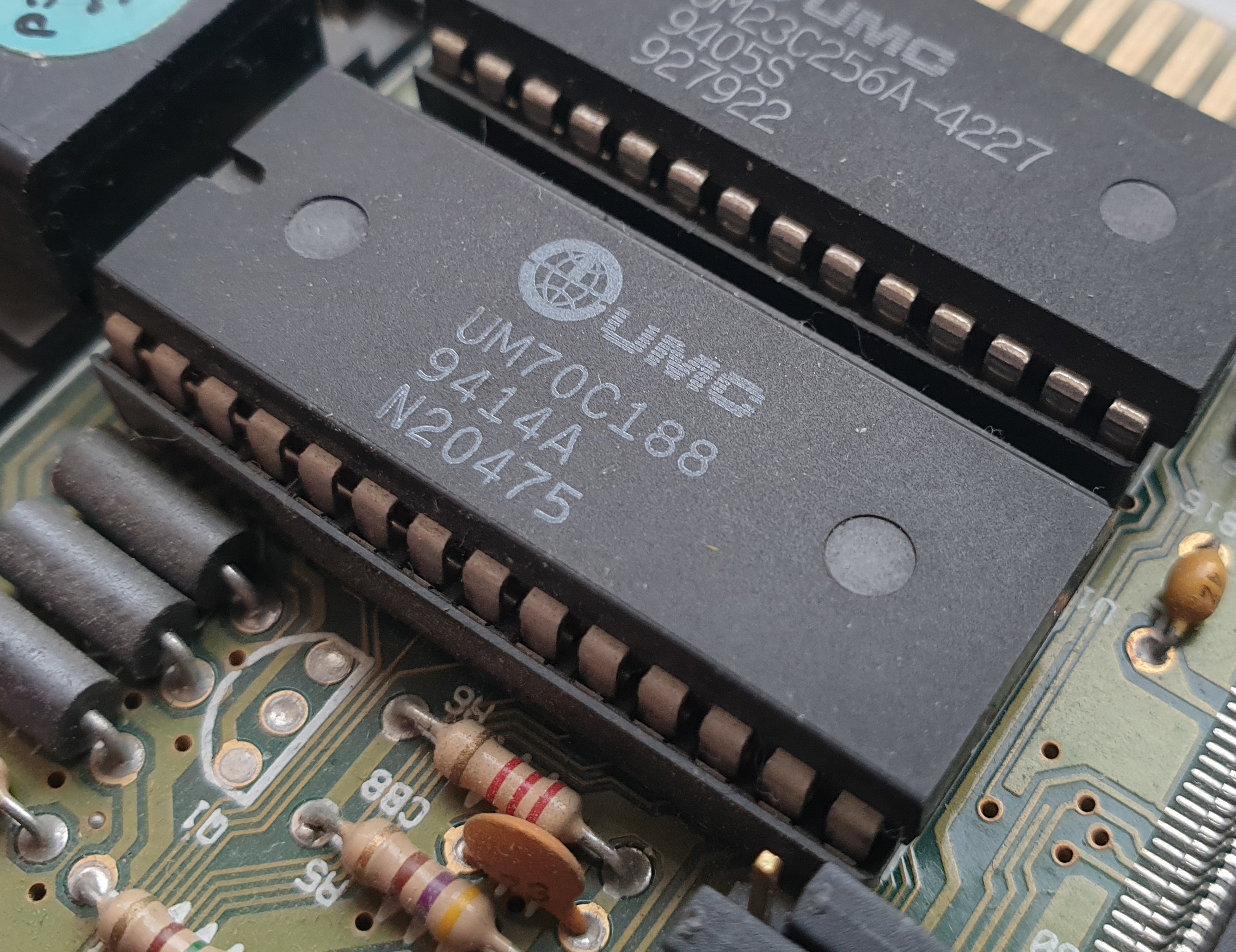 The RAMDAC on my card is the UM70C188 in a 28-pin DIP. Similar cards often have the UM70C178, and there are also a few that use a UM70C171.
Again, there are no datasheets available for these, but further research has uncovered the following:
The UM70C188 is a TrueColor (24-bit) RAMDAC.
The UM70C178 is a HiColor (15 or 16-bit) RAMDAC.
The UM70C171 is a 256 colour RAMDAC.
This UM70C188 is therefore functionally similar to the Sierra SC15025 or SC15026. Another card almost identical to mine used the Sierra SC11487 (a HiColor DAC).
Video Memory
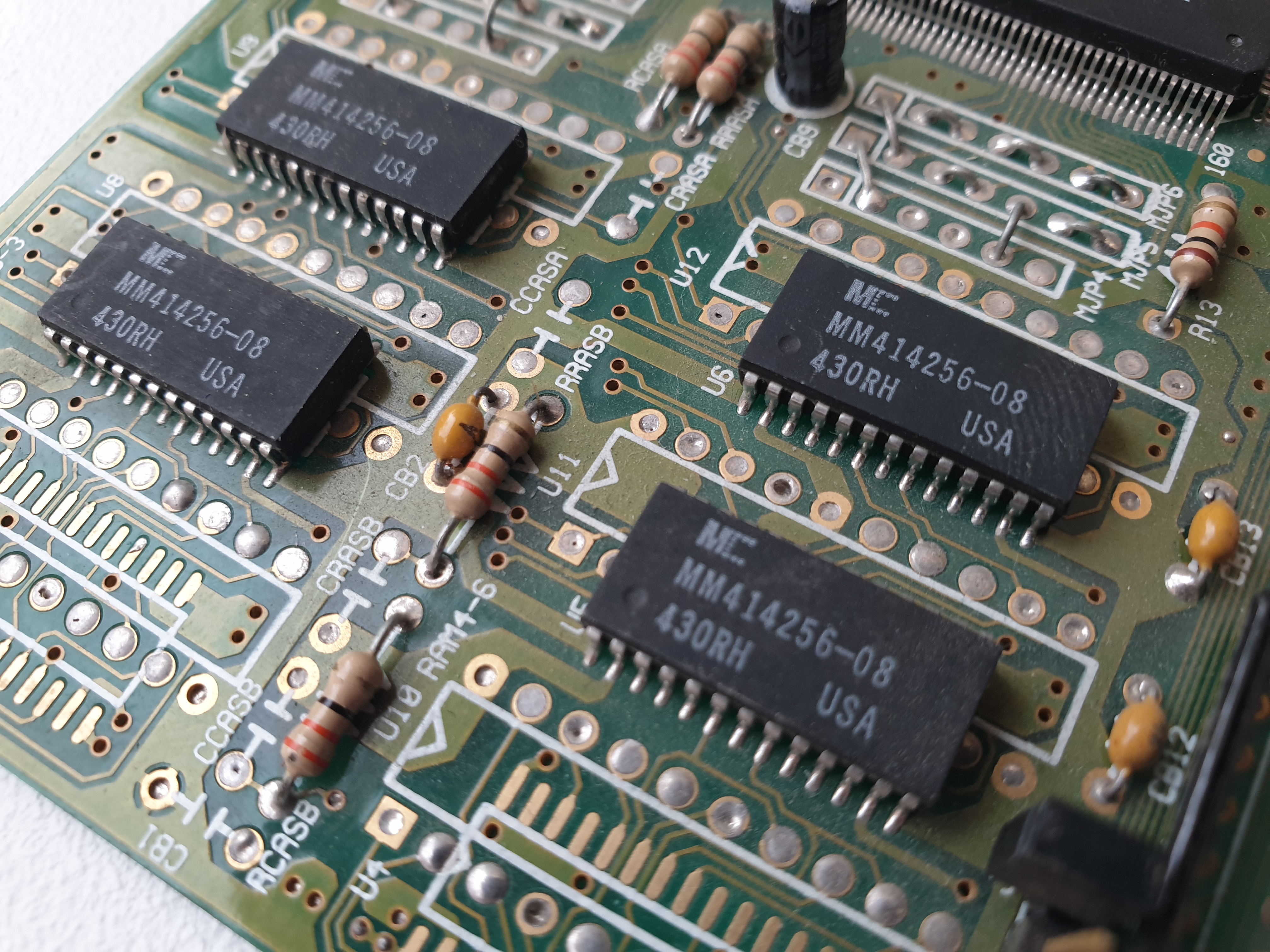 The UMC chipset supports memory sizes of 256 KB, 512 KB and 1 MB. This SVGA card has four MC-branded MM414256-08 DRAM chips which are 256 Kbit x 4, resulting in a total memory capacity of 512 KB. They are all rated for a middle-of-the-road 80ns access time.
A 512 KB VGA card would imply this card supports the following resolutions and colour depths:
- 1024 x 768 in 16 colours (4 bits per pixel)
- 800 x 600 in 256 colours (8 bits per pixel)
- 320 x 200 in 16.7 million colours (24 bits per pixel)
If the card had the full 1 MB it could do 640 x 480 in 16.7m colours.
The card appears to have solder pads for both the higher- and lower-profile DRAM chips, so it would be possible to upgrade this to the full 1 MB with some soldering work. It's likely though that other aspects of the card or the ISA bus itself would be a bottleneck. There is also the option on some motherboards to overclock the ISA bus, which I will also do to test how this card copes with a faster bus.
Crystal Oscillator and Clock Generator
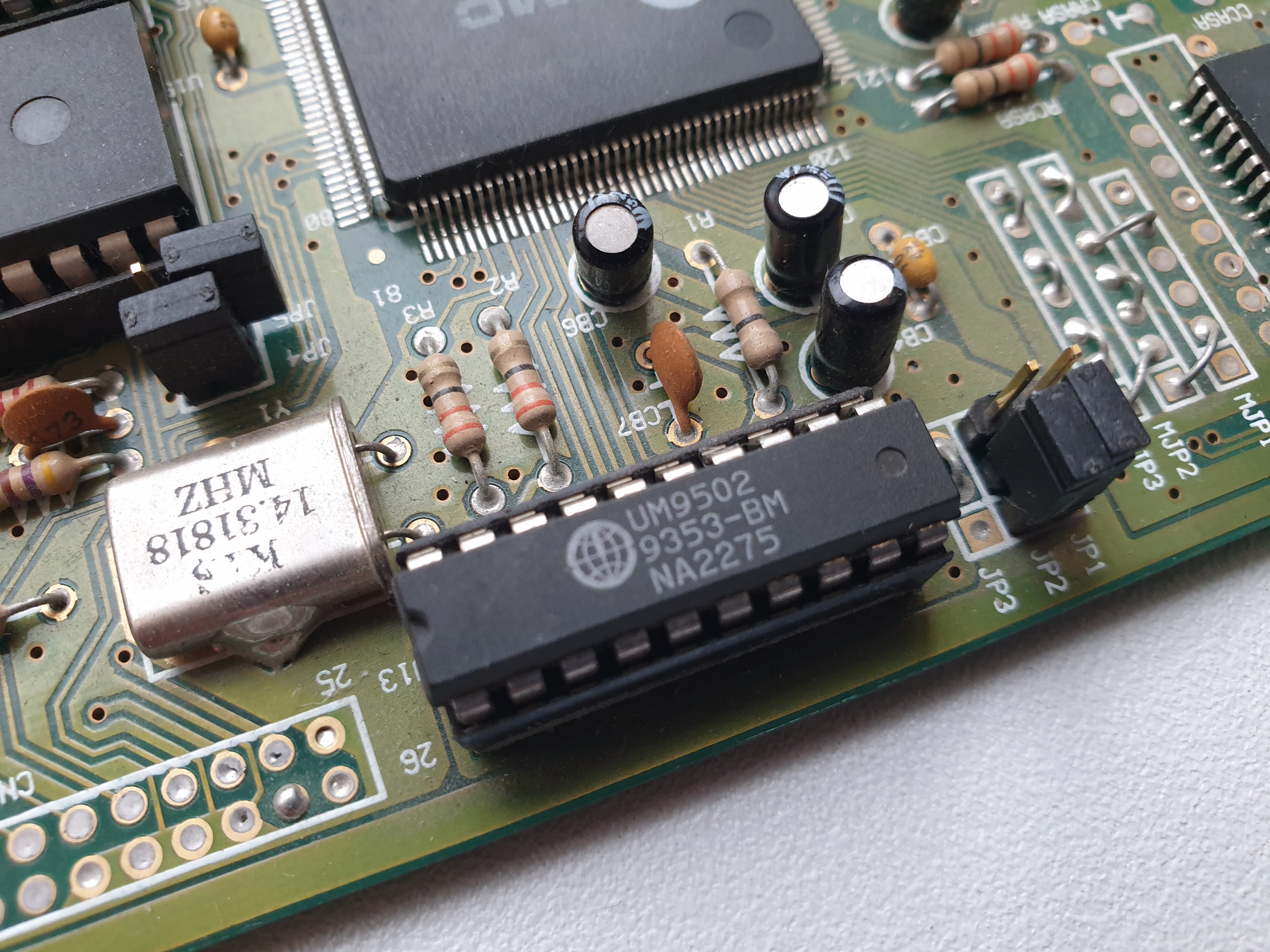 There is one crystal oscillator on the card, which runs at 14.31818 MHz and a UMC UM9502 video clock generator IC. The crystal would be used as the clock generator's input clock from which it would output numerous other clock signals.
Unlike EGA cards that often had multiple crystal oscillators to run at different pixel clocks (dot clocks) / refresh rates, a clock generator IC produces a variety of clock sources to handle all the frequencies of the many different display modes it supports. I will need some software to confirm the clock outputs generated, but they likely include 25.175 MHz (for VGA mode), 28.322 MHz (for VGA and CGA modes), 32.514 MHz (for EGA mode), and 40.0 MHz (for "Extended" modes).
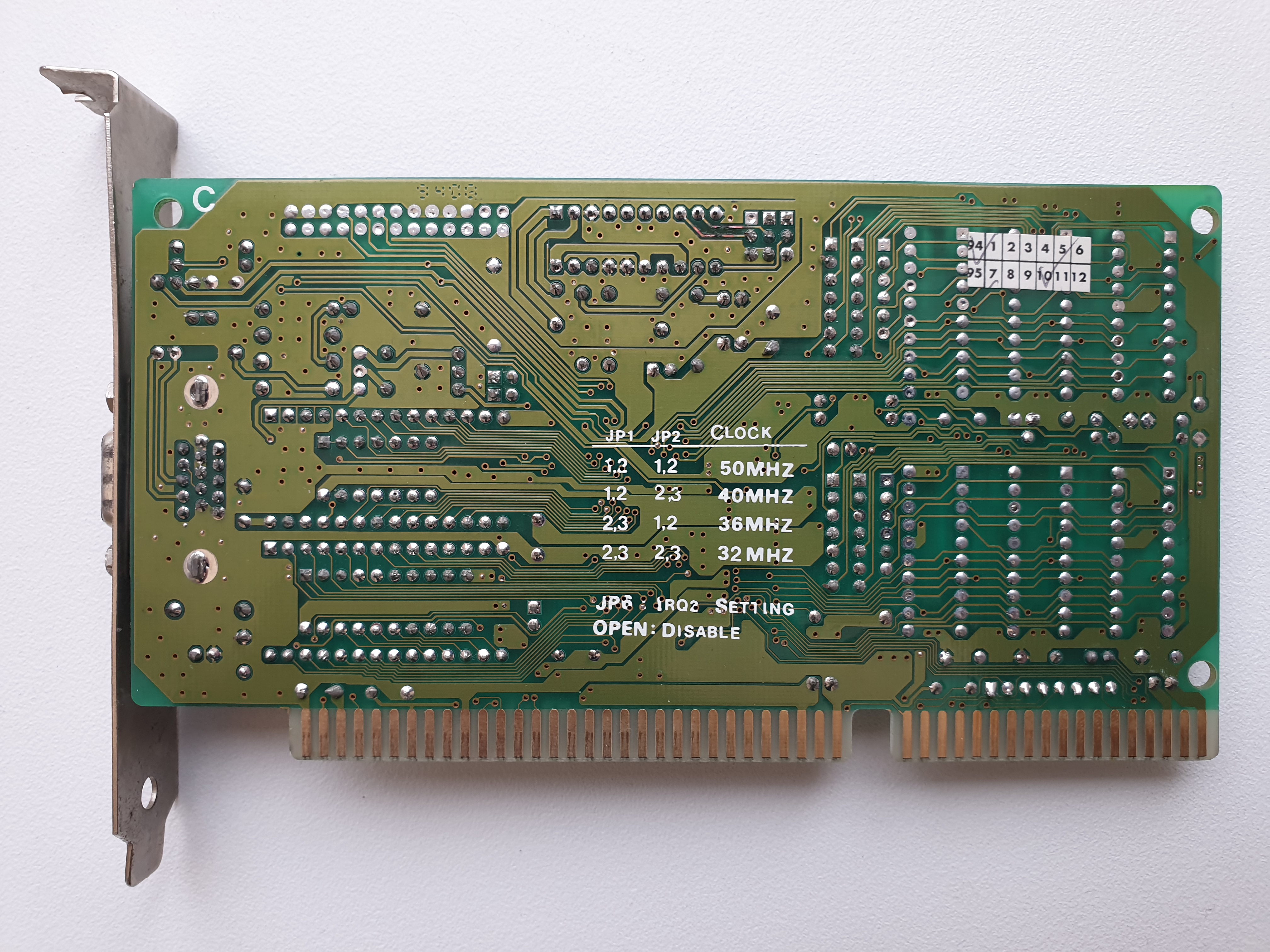
Jumpers
The card has six locations for jumpers, though only JP1-JP2, JP4-JP5 and JP6 actually have pin headers. JP3 is soldered closed 2-3
On the rear of the card, the silkscreen tells us what some of these are for, and I will take a guess at the others:
| Jumper | Meaning | Configuration |
|---|---|---|
| JP1, JP2 | Core clock (1-2 is toward the top of the card) | 50 MHz (JP1=1-2, JP2=1-2)* 40 MHz (JP1=1-2, JP2=2-3) 36 MHz (JP1=2-3, JP2=1-2) 32 MHz (JP1=2-3, JP2=2-3) |
| JP3 | Also connected to the clock - different multipliers? | 1-2 bridged* |
| JP4, JP5 | Type of RAMDAC installed? All cards with UM70C178 have JP4 open/JP5 closed. Another UM70C188 card has both open | JP4=Open, JP5=Open JP4=Closed, JP5=Open* |
| JP6 | IRQ2 enable/disable** | Closed (Enable) Open (Disable)* |
* = my card's settings
** = if enabled, this will fail to POST unless you go to your CMOS setup and set IRQ9 to 'Legacy ISA' first
In Part 2, I will test the card is fully functional and run some benchmarks to see what we can get out of it.