PC Chips M919 Motherboard - Part 1
13th June 2023
This rather famous PC Chips motherboard has been in my collection since September 2014, having acquired it in a bundle at auction for £48. Also included was a Dash 286 motherboard, AMD Am5x86 CPU, some memory, an MFM disk controller, some video cards, a floppy drive and a CD-ROM drive. The M919 was also sold by Amptron as the "DX9700". It is an interesting one in that it has VESA Local Bus, ISA, and PCI slots - often given the abbreviation of VIP because of this.
Around the time when this motherboard came out (1996), we were all transitioning from VL Bus to PCI, but it was actually fairly rare to have all of these buses on the same board as they sometimes didn't play well together. Here's a pic of an earlier version of the M919 with real cache chip slots and no COAST slot:

PC Chips M919 Rev 1.5 motherboard (1996)
Quick Visual Inspection
Looking around the board it appears to comprise the following:
|
|
The board layout is pretty good, but suffers from the common Socket 3 board issue where the location of the CPU with a heatsink/fan attached means two of the ISA slots become only usable by really short cards, and one of the PCI slots may well also fall foul of this if it's a really long PCI card. On the plus side, the cache slot is offset well enough to not be a problem.
Date-wise, the most recent date stamp on the motherboard's chips is week 22 of 1996, which is one of the UM8881/8886 chipset chips. This date stamp puts the motherboard's manufacture around 2nd June 1996.
The M919 came in numerous revisions - this particular one is V3.3B/F.
V1.2
- Four 72-pin SIMM slots and no 30-pin slots. No EDO support.
- Eight 32-pin SRAM cache sockets plus one 32-pin TAG RAM socket - no fake cache chips and no cache slot. 0/128/256/512/1024 KB.
- FSB speeds of 25 MHz and 33 MHz only.
- CPU speeds from 25 MHz up to 133 MHz, with 3.3V, 4.0V and 5V voltage settings
- Serial port problems/corruption/CMOS settings have no effect on it.
- Secondary IDE port non-functional/unreliable.
V1.4
- Unknown changes over V1.2.
V1.5
- FSB speeds of 40 MHz and 50 MHz added
- EDO RAM supported on some boards (must have an 'E' after the date stamp on the UM8881F)
V3.2
- First version with fake cache chips (two black plastic squares), but a new cache slot added. Only 256 KB cache supported.
- Two 72-pin SIMM slots and four 30-pin slots. Board arrangement changed to suit. Max. RAM is reduced from 256 MB to 128 MB.
- EDO RAM supported on some boards (must have an 'E' after the date stamp on the UM8881F)
- COM port issues fixed.
V3.3B/F
- Unknown changes over V3.2
V3.4B/F
- Fake cache chips removed (solder pads for them remain)
- Reverted back to having four 72-pin SIMM slots and no 30-pin slots.
The Component Parts
The CPU Socket
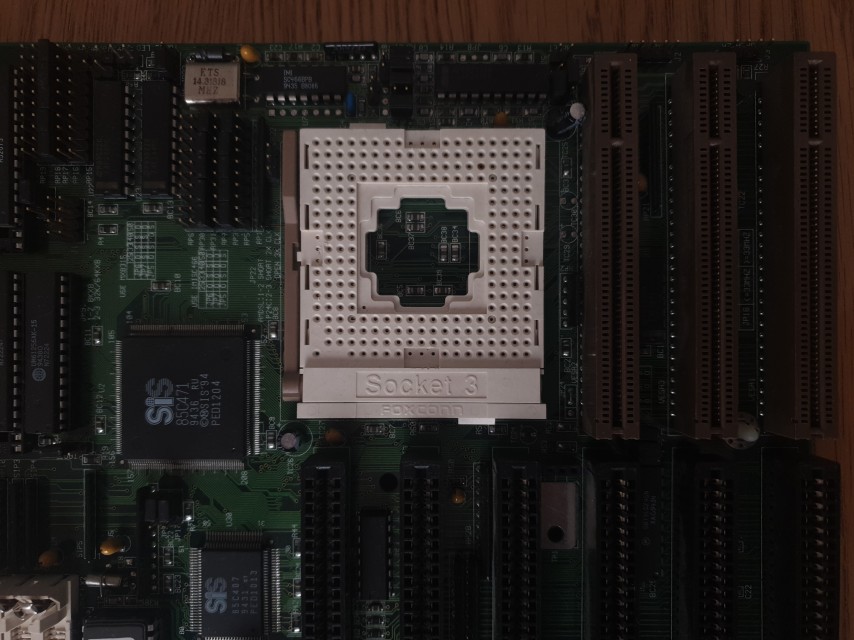 Being a Socket 3 motherboard and the presence of VESA Local Bus and PCI together puts this board late in the 486-era. As such it supports both 3.3V and 5V CPUs, selectable via jumpers on the board. The available CPU options are many, with clock speeds from 25 MHz up to 133 MHz:
From Intel: 80486SX, P23S (486SX SL Enhanced), DX, DX2, DX4, P24D (DX2 with Write-back Enhanced), P24T (486DX4 OverDrive 5V), P24C (DX4 3.45V).
From AMD: Enhanced Am486DX2 and DX4, and 5x86.
From Cyrix (and other-branded equivalents from TI, IBM, and SGS): Cx486DX (M6), Cx486DX2 (M7), Cx486DX4, and Cyrix 5x86 (M1sc).
The M919 (with UM8881F-EYA variant) was almost the only board to directly support Cyrix 5x86-specific features in the BIOS. The range of CPUs supported makes this a pretty useful motherboard to be installed in a retro PC if targeting anywhere in the 1989 to 1996 era.
The Chipset
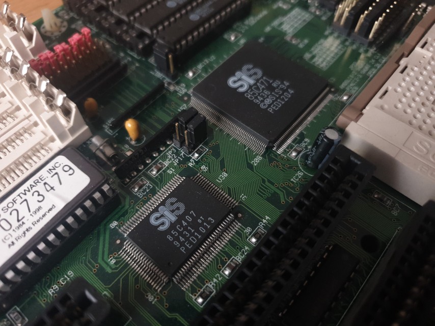 The motherboard uses the UMC UM8881F/8886BF chipset, launched in 1995. This was their late-486 chipset. This two-chip chipset consisted of:
- UM8881F - Northbridge (main CPU/memory/bus interface)
- UM8886BF - PCI-to-ISA bridge
In addition it used a UM8663BF which is the "Super I/O" chip responsible for the floppy disk controller, dual IDE controllers, two serial ports and a parallel port.
The chipset's key features include support for CPUs with a Write-Back L1 cache, up to 1 MB of L2 cache, and up to 256 MB of either Fast Page Mode main memory or EDO memory*.
There are at least three known revisions of the UM8881F "Northbridge" chip, denoted by the three letters after the date code. Those that start with 'B' are revision 1, and those with 'E' are revision 4. The next two letters are probably meaningless for our purposes and likely denote the type of chip/voltage/max. temperature tolerance. I put the earliest date code I could find for them in brackets to try to identify how early the B's and E's first arrived:
- BCA/BCS/BCT/BTA - FPM memory only supported (Week 11, 1995)
- ETA/ETO/ETS/ETT/EYA/EYS/EYT - added support for EDO memory and Cyrix 5x86 Linear Burst Mode (Week 48, 1995)
The Memory
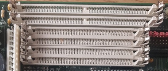 My revision of the motherboard replaced the four 72-pin slots with four 30-pin SIMM slots and two 72-pin SIMM slots, probably as a way to lure would-be upgraders to buy this motherboard so they didn't have to spend money on shiny new 72-pin SIMMs.
So we have three "banks" in all - Bank 0 is the 30-pin ones (called SIMM1 through SIMM4), with bank 1 (SIMM5) and bank 2 (SIMM6, closest to the edge of the board). Unlike most other boards, it will allow you to populate each of these banks independently, or use both bank 0 and bank 1. If populating only the 72-pin ones, you must start populating bank 1 before you populate bank 2.
The maximum amount of memory supported by the PC Chips M919 is a huge 256 MB.
30-pin SIMM modules that work are 256 KB, 1 MB, 4 MB, and 16 MB (note: no 8 MB support), though they must be 9-chip parity ones. For the 72-pin SIMM slots, you can use 256 KB, 1 MB, 2 MB, 4 MB, 8 MB, 16 MB or 32 MB modules - just make sure they are the same size if you are using them in addition to the 30-pin bank.
Level 2 Cache
This is where things get interesting. PC Chips became pretty famous for putting "fake" cache chips on some of their motherboards around this time. The M919 is no exception, having two black squares with traces that just go between them. Thankfully, they also provided a cache slot which can take a proprietary cache module (not Intel COAST standard). My M919 came with the 256 KB asynchronous write-back cache module, but PC Chips advertised several, including later pipelined cache ones that I'm pretty sure never actually got manufactured. This module is faster than the earlier V1.2 board revision's DIP cache chips.

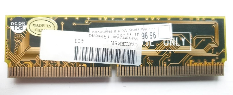
The proprietary PC Chips Asynchronous 256 KB Cache Module, front and rear.
The silkscreen text on the rear reads "For M919 Use Only"
The cache module I have comprises nine Alliance Semiconductor AS7C256 SRAM chips, eight of which gives us 256 KB of L2 cache with the ninth used for parity.
BIOS
My motherboard came with an American Megatrends WinBIOS 486 PCI/ISA BIOS, with a BIOS string of 41-P400-001437-00101111-101094-486AVIP-H. The 101094 tells us the core BIOS date of 10th October 1994. Looking on TheRetroWeb.com website for other BIOS', it appears this board had no other POST BIOS strings, but several BIOS versions were released:
2/16/95
11/08/95
2/16/96
3/6/96
4/15/96 - Plug & Play issues fixed - for earlier BIOS versions, use the Eurone PnP patch to fix it (pnpfix.zip).
5/6/96
5/31/96
The BIOS chip on my motherboard was rather difficult to identify. Under the AMI sticker the chip is stamped "M919 3-6" with a date code. Knowing the BIOS code is 128 KB in size, I removed the chip and put it into my EPROM programmer, trying to read the chip by choosing 128 KB EPROM chips I knew of, including the ST Microelectronics M27C1001, Winbond W9EE011, and Texas Instruments TMS27C010. None of these worked. Eventually I was able to read from the chip with the programmer configured for a Fujitsu MBM27C2001, which is a 256 KB chip. As expected, on this chip the code is simply written twice: once in the first 128 KB and again in the second 128 KB. You can download my BIOS dump, which is dated 6th March 1996 - notice the repeated code from 20000h.
<show BIOS startup POST codes and their descriptions>
<show boot-up screen>
<show BIOS screens>
VESA Local Bus Slots
The three VESA Local Bus slots are what I was keen on with the M919 - late 486 boards like this existed at a time when graphics performance was in real demand. Premium PCs that got the new Intel Pentium processor would have PCI slots and a PCI graphics card while these mid-range boards came with VLB and a VLB graphics card. The VESA Local Bus is able to drive a VLB graphics card at 33 MHz instead of the ISA bus's sedentary 8 MHz. Having PCI as well on the same board means I should be able to compare a whole load of my VLB and PCI video cards.
Quirks Galore
I have read of several anomalies with the M919, such as when using EDO RAM the Level 2 cache is disabled.
Another oddity of the board is that when you try to run a multiplier of 4x (I think), for example when running an AMD Am5x86-133. What is believed to occur is that the AMI WinBios must set things up based on the boot speed, so if you configure your CPU to run at 133 MHz the PCI bus speed will be 33 MHz, but using a 4x multiplier runs the CPU at 166 MHz, but the PCI bus is reduced to 20 MHz.
The cool hack is to setup your turbo switch to the 40 MHz FSB jumper, have the machine boot in the slow PCI mode and then activate your ‘turbo’ - it will then have the system work normally at the desired 4x CPU multiplier and possibly even overclocks your PCI bus to 40 MHz! This is because hot-switching after boot-up must keep the dividers disabled, so it's forced to run at the 166/4.
In Part 2, we'll get it operational using a period-correct CPU, a 486DX2-66, and get some early performance test results out of it, as well as checking out those quirks!